 |
FEEDBACK
AND OPERATIONAL AMPLIFIERS
(Some selected section from CHAPTER
3 of the book "The Art of Electronics", written by Paul Horowitz and Winfield
Hill, Cambridge University Press , 1985.)
|
|
|
|
|
|
BASIC OP-AMP CIRCUITS |
|
|
COMPARATORS AND SCHMITT TRIGGER |
|
|
FEEDBACK WITH AMPLIFIERS |
|
|
FEEDBACK AMPLIFIER FREQUENCY COMPENSATION |
FEEDBACK WITH FINITE-GAIN AMPLIFIERS
We mentioned in Section 3.12
that the finite open-loop gain of an op-amp limits its ; performance in
a feedback circuit. Specifically, the closed-loop gain can never exceed
the open-loop gain, and as the open-loop gain approaches the closed loop
gain, the amplifier begins to depart from the ideal behavior we have come
to expect. In this section we ; will quantify these statements so that
you will be able to predict the performance of a feedback amplifier constructed
with real (less than ideal) components. This is important also for feedback
amplifiers constructed entirely with discrete components (transistors),
where the open-loop gain is usually much less than with op-amps. In these
cases the output impedance, for instance, will not be zero. Nonetheless,
with a good understanding of feedback principles you will be able to achieve
the performance required in any given circuit.
 |
.
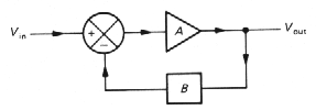
Figure 3-58 |
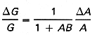
3.24 Gain equation
Let's begin by considering an amplifier
of finite voltage gain, connected with feedback (Fig. 3.58). The amplifier
has open-loop voltage gain A, and the feedback network subtracts a fraction
B of the output voltage from the input. (Later we will generalize things
so that inputs and outputs can be currents or voltages.) The input to the
gain block is then Vin - BVout.But the output
is just the input times A:
| A (Vin - B Vout) = Vout |
In other words,
 |
 |
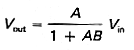
Some terminology: The standard designations
for these quantities are as follows:
G = closed-loop gain,
A = open-loop gain,
AB = loop gain,
1 + AB = return difference, or desensitivity.
The feedback network i sometimes called
the beta network (no relation to transistor beta, hfe,bF).
3.25 Effects of feedback
on amplifier circuits
Let's look at the important effects of
feedback. The most significant are predictability of gain (and reduction
of distortion changed input impedance, and change output impedance.
Predictability of gain
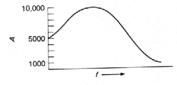
The voltage gain is A/(1 + AB). In the limit of infinite open-loop gain A, G = 1 /B. We saw this result in the noninverting amplifier configuration, where a voltage divider on tl output provided the signal to the inverting input. The closed-loop voltage gain was just the inverse of the division ratio of the voltage divider. For finite gain A, feedback still acts to reduce the effects of variations of A (with frequency, temperature,amplitude, etc.). For instance, suppose A depends frequency as in Figure 3.59.
 |
.
Figure 3-59 |
It is easy to show that relative variations in the open-loop gain are reduced by the desensitivity:
 |
A very important consequence of this is that nonlinearities, which are simply gain variations that depend on signal level, are reduced in exactly the same way.
Feedback can be arranged to subtract a voltage or a current from the input (these are sometimes called series feedback and shunt feedback, respectively). The noninverting op-amp configuration, for instance, subtracts a sample of the output voltage from the differential voltage appearing at the input, whereas in the inverting configuration a current is subtracted from the input. The effects on input impedance are opposite in the two cases: Voltage feedback multiplies the open-loop input impedance by 1 + AB, whereas current feedback reduces it by the same factor. In the limit of infinite loop gain the input impedance (at the amplifier's input terminal) goes to infinity or zero, respectively. This is easy to understand, since voltage feedback tends to subtract signal from the input, resulting in a smaller change (by the factor AB)across the amplifier's input resistance; it's a form of bootstrapping. Current feedback reduces the input signal by bucking it with an equal current.
 |
.
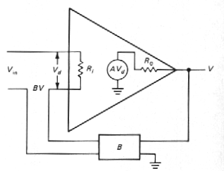
Figure 3-60 |
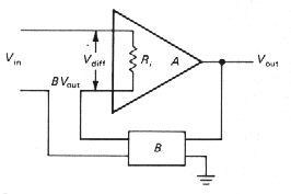
Let's see explicitly how the effective input impedance is changed by feedback. We will illustrate the case of voltage feedback only, since the derivations are similar for the two cases. We begin with an op-amp model with (finite) input resistance as shown in Figure 3.60. An input Vin is reduced by BVout , putting a voltage Vdiff=V1-BVout across the inputs of the amplifier. The input current is therefore
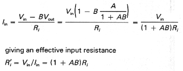 |
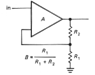
The classic op-amp noninverting amplifier is exactly this feedback configuration, as shown in Figure 3.61. In this circuit, B = R1 /(R1 + R2), giving the usual voltage gain expression Gv= 1 + R2 /R1 and an infinite input impedance for the ideal case of infinite open-loop voltage gain A. For finite loop gain the equations as previously derived apply.
 |
.
Figure 3-61 |
In the case of current (shunt) feedback, the input to the amplifier is at the "summing junction'" (the inverting input of the amplifier), where the currents from feedback and input signals are combined (this amplifier connection is really a "transresistance" configuration; it converts a current input to a voltage output). Feedback reduces the impedance looking into the summing junction (including the resistance of the feedback resistor) by the factor 1 + AB. In cases of very high loop gain (e.g., an op-amp) the input impedance is reduced to a fraction of an ohm, a good characteristic for a current-input amplifier. Some good examples are the photometer amplifier in Section 3.21.
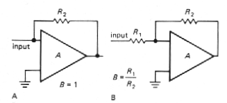 |
Figure 3-62 Input impedance of the inverting amplifier |
The classic op-amp inverting amplifier connection is a combination of a shunt feedback amplifier and a series input resistor, as shown in Figure 3.62. As a result, the input impedance equals the sum of R1, and the impedance looking into the summing junction. For the ideal case of infinite open-loop voltage gain, the input impedance of the entire amplifier circuit is just R1, and the gain is -R2/R1.
 |
.
Figure 3-63 |
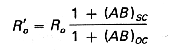
Again, feedback can extract a sample of the output voltage or the output current. In the first case the open-loop output impedance will be reduced by the factor 1 + AB, whereas in the second case it will be increased by the same factor. We will illustrate this effect for the case of voltage sampling. We begin with the model shown in Figure 3.63. This time we have shown the output impedance explicitly. The calculation is simplified by a trick: Short the input, and apply a voltage V to the output; by calculating the output current I, we get the output impedance R'o = V/I. Voltage V at the output puts a voltage -BV across the amplifier's input, producing a voltage -ABVin the amplifier's internal generator. The output current is therefore
 |
If feedback is connected instead to sample
the output current, the expression becomes
| R'o = Ro(1 + AB) |
It is possible to have multiple feedback paths, sampling both voltage and current. In the general case the output impedance is given by Blackman's impedance relation
 |
l Loading by the feedback network
In feedback computations, you usually assume that the beta network doesn't load the amplifier's output. If it does, that must be taken into account in computing the open-loop gain. Likewise, if the connection of the beta network at the amplifier's input affects the open-loop gain (feedback removed, but network still connected), you must use the modified open-loop gain. Finally, the preceding expressions assume that the beta network is unidirectional, i.e., it does not couple signal from the input to the output.
F Vplyv spätnej väzby na vlastnosti zosilňovača (zhrnutie)
13.26 Two examples of
transistor amplifiers with negative feedbacks
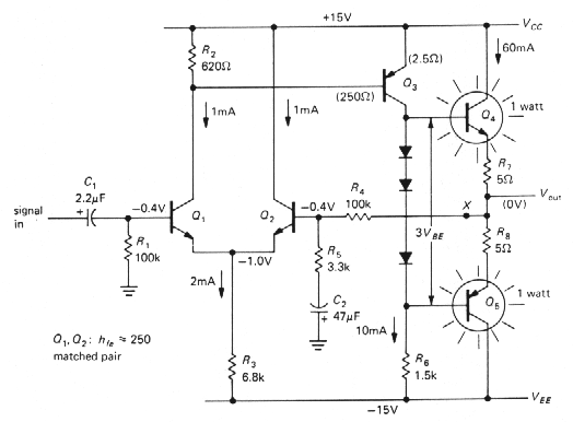
Figure 3.64 shows a transisotr amplifier with negative feedback.
 |
.
Figure 3-64 Transistor power amplifier with negative feedback |
l Circuit description
It may look complicated, but it is extremely straightforward in design and is relatively easy to analyze. Q1 and Q2 form a differential pair, with common-emitter amplifier Q3 amplifying its output. R6 is Q3's collector load resistor, and push-pull pair Q4 and Q5 form the output emitter follower. The output voltage is sampled by the feedback network consisting of voltage divider R4 and R5, with C2 included to reduce the gain to unity at dc for stable biasing. R3 sets the quiescent current in the differential pair, and since overall feedback guarantees that the quiescent output voltage is at ground, Q3's quiescent current is easily seen to be 10mA (VEEacross R6, approximately). The diodes bias the push-pull pair into conduction, leaving one diode drop across the series pair R7, and R8, i.e., 60mA quiescent current. That's class AB operation, good for minimizing crossover distortion, at the cost of 1 watt standby dissipation in each output transistor.
From the point of view of our earlier circuits,
the only unusual feature is Q1's quiescent collector voltage,
one diode drop below VCC. That is where it must sit in
order to hold Q3 in conduction, and the feedback path ensures
that it will. (For instance, if Q1 were to pull its collector
closer to ground, Q3 would conduct heavily, raising the output
voltage, which in turn would force Q2 to conduct more heavily,
reducing Q1's collector current and hence restoring the status
quo.) R2 was chosen to give a diode drop at Q1's
quiescent current in order to keep the collector currents in the differential
pair approximately equal at the quiescent point. In this transistor circuit
the input bias current is not negligible (4mA), resulting in a 0,4 volt
drop across the 100k input resistors. In transistor amplifier circuits
like this, in which the input currents are considerably larger than in
op-amps, it is particularly important to make sure that the dc resistances
seen from the inputs are equal, as shown (a Darlington input stage would
probably be better here).
l Analysis
Let's analyze this circuit in detail, determining the gain, input and output impedances, and distortion. To illustrate the utility of feedback, we will find these parameters for both the open-loop and closed-loop situations (recognizing that biasing would be hopeless in the open-loop case). To get a feeling for the linearizing effect of the feedback, the gain will be calculated at +10 volts and -10 volts output, as well as the quiescent point (zero volts).
l Open loop
Input impedance: We cut the feedback at point X and ground the right side of R4. The input signal sees 100k in parallel with the impedance looking into the base. The latter is hfe times twice the intrinsic emitter resistance plus the impedance seen at Q2's emitter due to the feedback network at Q2's base. For hfe ~ 250, Zin~ 250 X[(2 X 25) + (3.3k/250)]; i.e., Zin~ 16k.
Output impedance: Since the impedance looking back into Q3's collector is high, the output transistors are driven by a 1.5k source (R6). The output impedance is about 15 ohms (hfe ~ 100) plus the 5 ohm emitter resistance, or 20 ohms. The intrinsic emitter resistance of 0.4 ohm is negligible.
Gain: The differential input stage sees a load of R2 paralleled by Q3's base resistance. Since Q3 is running 10mA quiescent current, its intrinsic emitter resistance is 2.5 ohms, giving a base impedance of about 250 ohms (again, hfe ~ 100). The differential pair thus has a gain of
| 250 || 620 or
3.5
2 x 25W |
The second stage, Q3, has a
voltage gain of 1.5k/2.5 ohms, or 600. The overall voltage gain at the
quiescent point is 3.5 x 600, or 2100. Since Q3's gain depends
on its collector current, there is substantial change of gain with signal
swing, i.e., nonlinearity. The gain is tabulated in the following section
for three values of output voltage.
l Closed Ioop
Input impedance: This circuit uses series feedback, so the input impedance is raised by (1 + loop gain). The feedback network is a voltage divider with B= 1 /30 at signal frequencies, so the loop gain AB is 70. The input impedance is therefore 70 x 16k, still paralleled by the 100k bias resistor, i.e., about 92k. The bias resistor now dominates the input impedance.
Output impedance: Since the output voliage is sampled, the output impedance is reduced by (1 + loop gain). The output impedance is therefore 0.3 ohm. Note that this is a small-signal impedance and does not mean that a 1 ohm load could be driven to nearly full swing, for instance. The 5 ohm emitter resistors in the output stage limit the large signal swing. For instance, a 4 ohm load could be driven only to 10 volts pp, approximately.
Gain: The gain is A/(1 + AB). At the quiescent point that equals 30.84, using the exact value for B. In order to illustrate the gain stability achieved with negative feedback, the overall voltage gain of the circuit with and without feedback is tabulated at three values of output level at the end of this paragraph. It should be obvious that negative feedback has brought about considerable improvement in the amplifier's characteristics, although in fairness it should be pointed out that the amplifier could have been designed for better open-loop performance, e.g., by using a current source for Q3's collector load and degenerating its emitter; by using a current source for the differential pair emitter circuit, etc. Even so, feedback would still make a large improvement.
 |
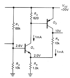
l Series feedback pair
Figure 3.65 shows another transistor amplifier with feedback. Thinking of Q1 as an amplifier of its base-emitter voltage drop (thinking in the Ebers-Moll sense), the feedback samples the output voltage and subtracts a fraction of it from the input signal. This circuit is a bit tricky because Q2's collector resistor doubles as the feedback network. Applying the techniques we used earlier, you should be able to show that G (open loop) ~ 200, loop gain ~ 20, Zout (open loop) ~ 10k, Zout (closed loop) ~ 500 ohms, and G (closed loop) ~ 9.5.
 |
.
Figure 3-65 |
| Back to menu |