| Amplifier pass-band |
In most amplifiers applications we want fidelity of amplification (=>output wave shape identical to the input shape form). If the input signal is non-sinusoidal (the principles of Fourier analysis show that such signal consist of broad spectrum of harmonically related frequencies) to achieve undistorted output all component frequencies (to 3 - 5 harmonics of repetition frequency) must be equally amplified in magnitude.
Unequal gain for the frequency components causes (gain - frequency curve and phase - frequency curve)) distortion.
In middle-frequency range the gain and phase angle are reasonable constant => circuits reactances have negligible effect (series-capacitive reactances approximate short circuits, all shunt-capacitive reactances appear as effective open circuits)
In high-frequency range shunt capacitance (result of the internal transistor capacitance) reduces the load impedance and output voltage.
In low-frequency range the series capacitance increase in reactance and progressively cause a drop in the response with falling frequency.
The amplifier bandwidth BW=fH0-fL0since
the low frequency limit BW can be extended to zero frequency, the high-frequency
limit restricts the amplifier bandwidth.
Fig. 3-85
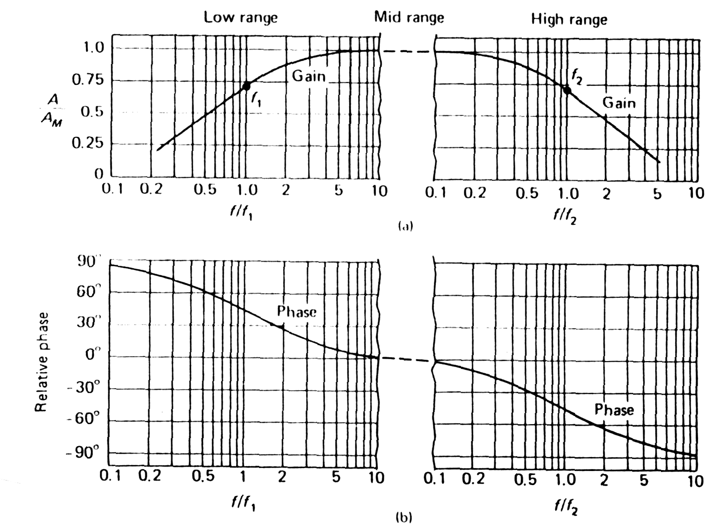 |
Fig. 3-85a |
Gain versus frequency curves driven in logarithmic scale are known as Bode plots => we can employ straight-line approximation to obtain the performance characteristic corner frequency at which asymptotes of the dB curves intersect. => correction for curve in corner frequency (10 log2=3dB).
Gain-frequencies curves in dB being additive.
(The gain of 2-stage identical amplifier fall at -40dB per frequency decade
(12 dB per octave), 3-stage circuits will have a gain curve that falls
at -60dB per decade. The phase angle will be multiplied by the number
of stages +-90o and at extreme frequency in n-stage amplifier
=> critical condition for oscillation. When stages of the amplifier
are cascaded the bandwidth is reduced.
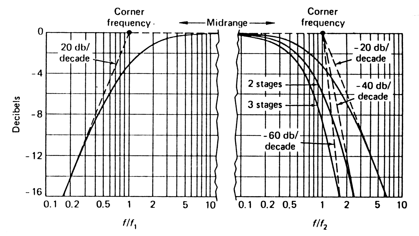 |
Fig. 3-85b
Response curves (3 stages amplifier) from Bode asymptotes. |
![]()
| Feedback |
Black box width feedback (voltage) illustrates
the sampling by the b
(beta) network and reverse transmissions of signal in feedback system.
(=> giving on output bU2
=> is subtracted from the voltage U1 at the mixing point, to
yield the error signal UD.
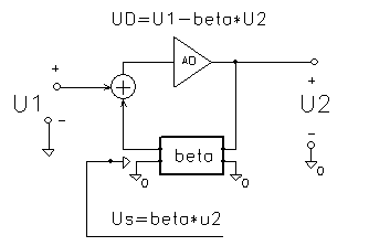 |
Fig. 3-80
Principle of the feed back |
Open-loop gain AD-
internal gain of the amplifier.
In sampling of the input voltage bU2
(on fig. beta*U2)
Closed-loop gain A=
AD/(1+bAD)~1/b.
Output sampling:
Output resistance in:
| voltage feedback | current feedback |
| R'0=R0/(1+bAD) | R'0=R0(1+bAD) |
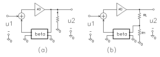 |
Fig. 3-81
Output sampling |
Effect of feedback on input resistance:
| Seriesinput: | Shunt input: |
| R'i=Ri(1+bAD) | R'i=Ri/(1+bAD) |
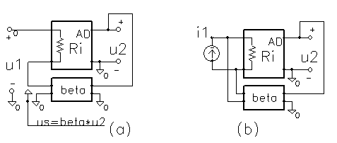 |
Fig. 3-82
Effect of feedback on input resistance |
![]()
| Applications examples of op amp |
Inverting op amp, non-inverting
op amp and the unity-gain buffer
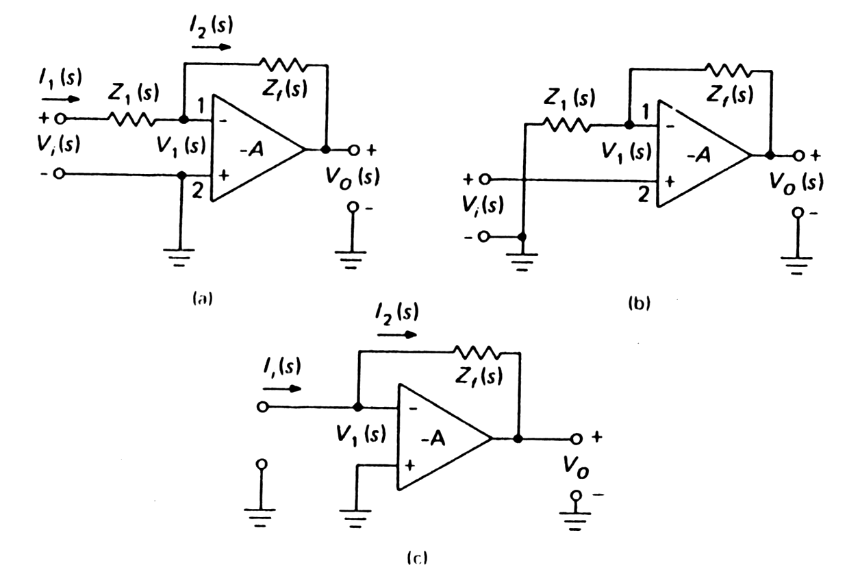 |
Fig. 3-83
Operational amplifier:
|
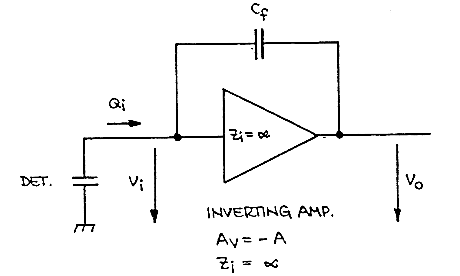
The integration operation amplifier (in fig (a)
above, if Zf is a capacitance will perform mathematical
operation of integration on the input signal). By considering property
of the integration operation amplifier the Miller effect can be explained
as increasing equivalent input capacitance C'=(1+AD)C and so
a very large time constant circuits can be achieved. Example of such a
circuit see active integrator called "charge sensitive
amplifier"
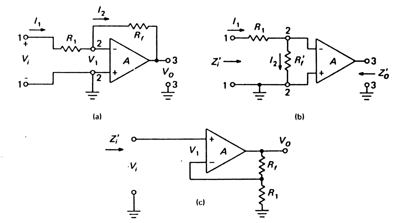 |
Fig. 3-84 Operational amplifier
|
The application of negative feedback to amplifiers is effective in increasing the amplifier bandwidth. In general, instability of the voltage feedback never differs as much as 180o from its middle-range => reduce by corrective RC circuits in 1 stage. The compensation network seriously reduces the amplifier bandwidth.
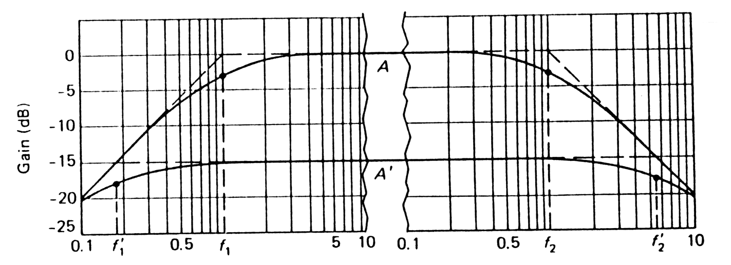 |
Fig. 3-85c
Constant gain-band-width product with 15-dB feedback => increasing the amplifier bandwidth. |
Monolithic construction, with a complete amplifier integrated into tiny silicon chip, leads very small size, balancing of temperature effects, reduced cost, and improved reliability by elimination of much interconnecting wiring.
By addition of negative feedback to a high-gain (A>5000) integrated amplifier => operational amplifier ("op-amp"). This circuits closely approaches an ideal package of gain, with high input resistance and low output resistance.
Use of negative feedback
sacrifices gain, reduce distortion, improve stability
of gain, alter frequency response and modify
input and output impedance.
 |
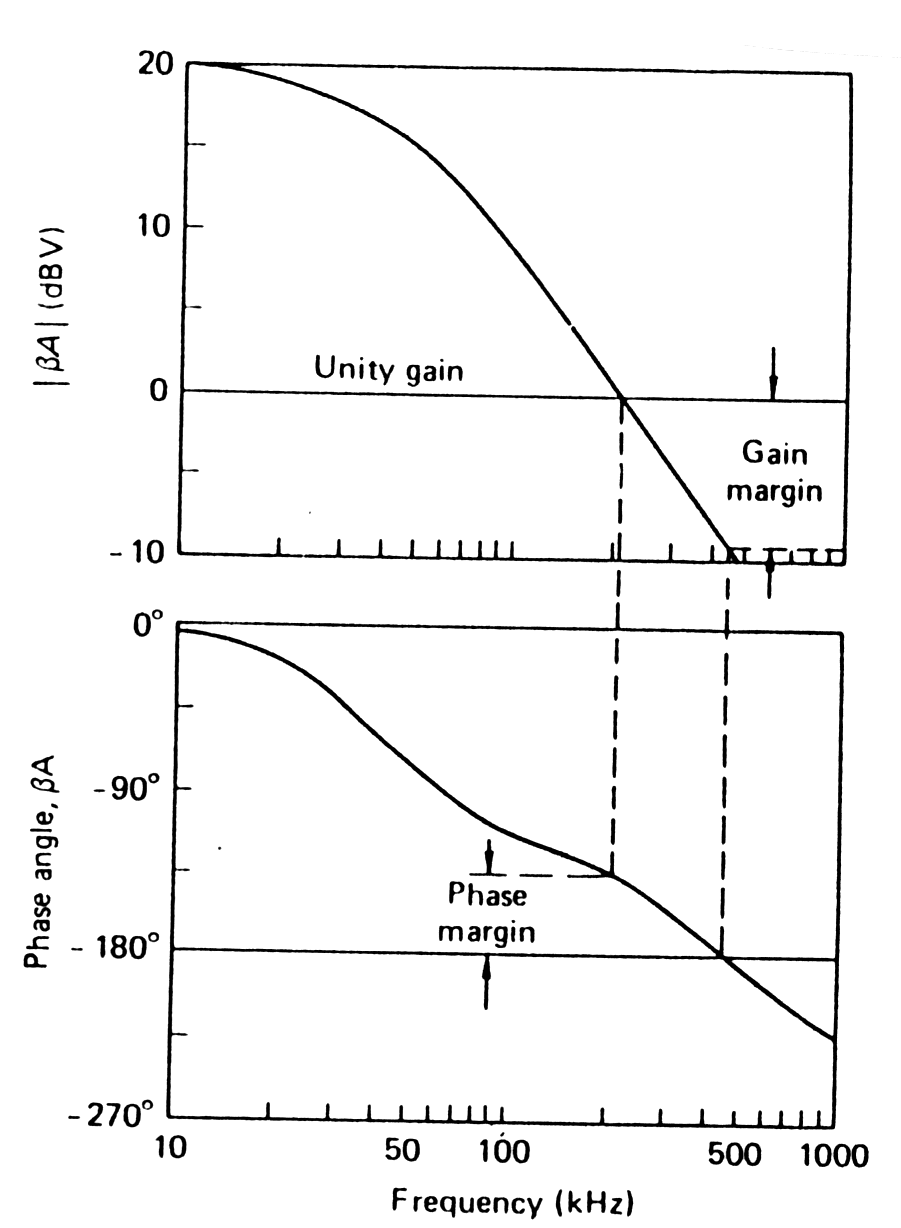 |
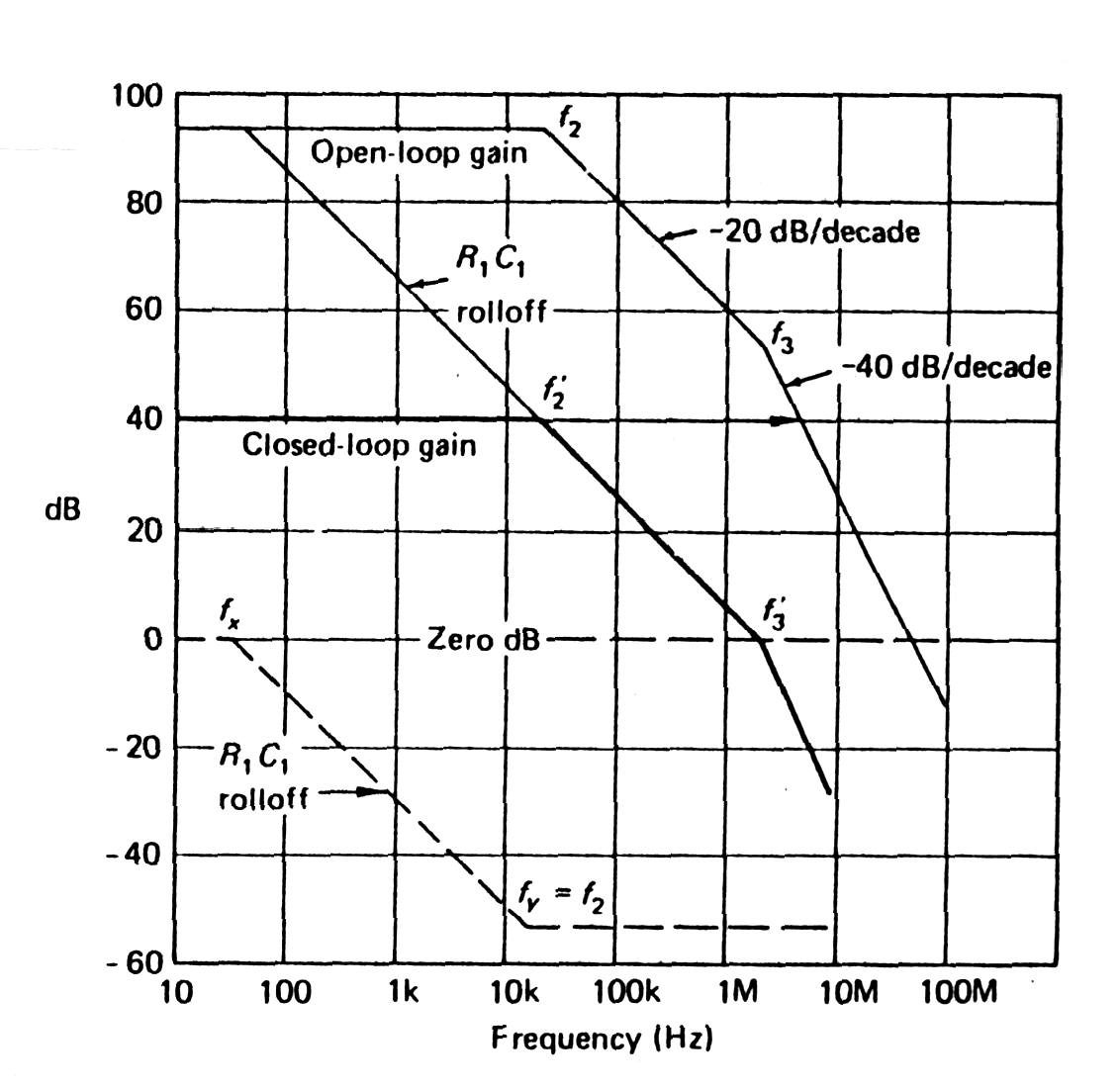
| Fig. 3-86 Example of compensation of 709 operational amplifier => reducing by corrective RC circuits the amplifier bandwidth. | Fig. 3-87 Gain and phase margins after correcting with RC circuits. |
![]()
| Capacitance of the pn-junction |
When a pn-junction is under reverse voltage UD (case of semiconductor detector) the transition region is depleted of mobile charges (=> More mobile charge is removed and the depleted region increases whit increasing UD) and takes on the properties of a dielectric, with only fixed charges present.
The dynamic transition capacitance depends on r.m.s. of applied voltage (UB+UD)~UD, where UB - barrier potential of junction, UD - applied outside voltage:
To make charge response independent of variance
in detector capacitance is necessary use active
integrator called "charge sensitive amplifier"
 |
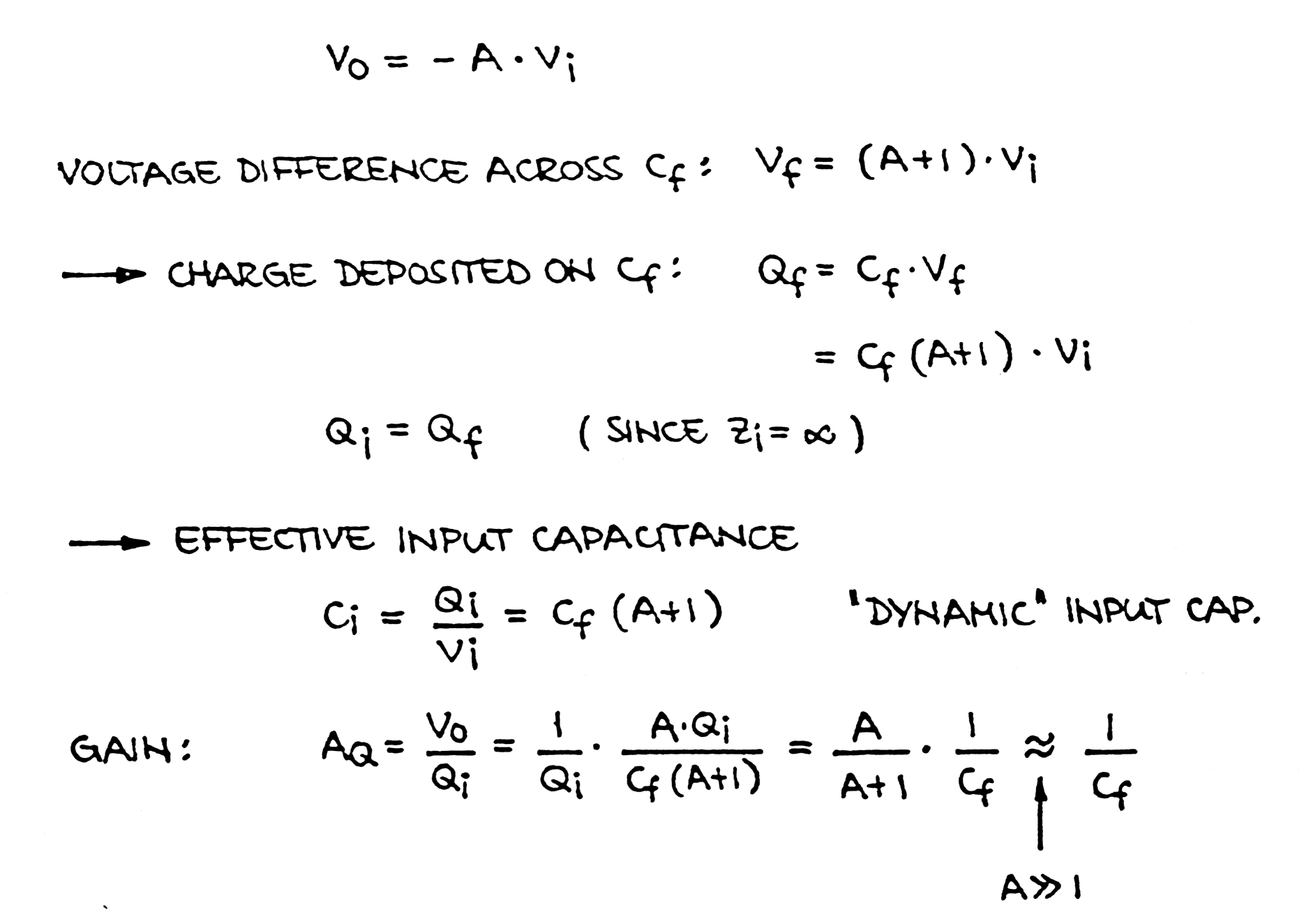 |
| Fig. 3-84 Active integrator called "charge sensitive amplifier". The gain AQ ~ 1/Cf depnds on the feedback capacitance Cf and did not depnds on capacitance Cdet of the semiconductor detector. | |
![]()
|
|
Back to previous page |