 |
FEEDBACK AND OPERATIONAL AMPLIFIERS
(Some selected
section from CHAPTER 3 of the book "The Art of Electronics", written by
Paul Horowitz and Winfield Hill, Cambridge University Press , 1985.) |
|
|
|
|
|
BASIC OP-AMP CIRCUITS |
|
|
COMPARATORS AND SCHMITT TRIGGER |
|
|
FEEDBACK WITH AMPLIFIERS |
|
|
FEEDBACK AMPLIFIER FREQUENCY COMPENSATION |
![]()
INTRODUCTION TO FEEDBACK AND OPERATIONAL AMPLIFIERS
Feedback has become such a well-known
concept that the word has entered the general vocabulary. In control
systems, feedback consists in comparing the output of the system with
the desired output and making a correction accordingly. The "system"
can be almost anything: for instance, the process of driving a car down
the road, in which the output (the position and velocity of the car) is
sensed by the driver, who compares it with expectations and makes
corrections to the input (steering wheel, throttle, brake). In
amplifier circuits the output should be a multiple of the input, so in
a feedback amplifier the input is compared with an attenuated version
of the output.
3.01 Introduction to feedback
Negative feedback is the process of coupling the output back in such a way as to cancel some of the input. You might think that this would only have the effect of reducing the amplifier's gain and would be a pretty stupid thing to do. True, it does lower the gain, but in exchange it also improves other characteristics, most notably freedom from distortion and nonlinearity, flatness of response (or conformity to some desired frequency response), and predictability. In fact, as more negative feedback is used, the resultant amplifier characteristics become less dependent on the characteristics of the open-loop (no-feedback) amplifier and finally depend only on the properties of the feedback network itself. Operational amplifiers are typically used in this high-loop-gain limit, with open-loop voltage gain (no feedback) of a million or so.
A feedback network can be frequency dependent, to produce an equalization amplifier (with specific gain-versus-frequency characteristics,), or it can be amplitude-dependent, producing a nonlinear amplifier (a popular example is a logarithmic amplifier). It can be arranged to produce a current source (near-infinite output impedance) or a voltage source (nearzero output impedance), and it can be connected to generate very high or very low input impedance. Speaking in general terms, the property that is sampled to produce feedback is the property that is improved. Thus, if you feed back a signal proportional to the output current, you will generate a good current source.
Feedback can also be positive; that's how you make an oscillator, for instance. As much fun as that may sound, it simply isn't as important as negative feedback. More often it's a nuisance, since a negative feedback circuit may have large enough phase shifts at some high frequency to produce positive feedback and oscillations. It is surprisingly easy to have this happen, and the prevention of unwanted oscillations is the object of what is called compensation.
Having made these general comments, we will now look at a few feedback examples with operational amplifiers.
FPrincíp spätnej
väzby v zosilňovači
3.02 Operational amplifiers
Most of our work with feedback will involve
operational amplifiers, very high gain dc-coupled differential
amplifiers with singleended outputs. [You can think of the classic
differential amplifiers with its two inputs and single output as a
prototype, although real op-amps have much higher gain (typically 105
to 106) and lower output impedance and allow the output to swing
through most of the supply range (you usually use a split supply, most
often ± 15V)]. Operational amplifiers are now available in literally
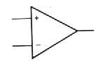
hundreds of types, with the universal symbol shown in Figure 3.1, where
the (+) and (-) inputs do as expected: The output goes positive when
the noninverting input (+) goes more positive than the inverting input
(-), and vice versa. The (+) and (-) symbols don't mean that you have
to keep one positive with respect to the other, or anything like that;
they just tell you the relative phase of the output (which is important
to keep negative feedback negative). Using the words "noninverting" and
"inverting," rather than "plus" and "minus," will help avoid confusion.
Power-supply connections are frequently not displayed, and there is no
ground terminal. Operational amplifiers have enormous voltage gain, and
they are never used without feedback. Think of an op-amp as
fodder for feedback. The open-loop gain is so high that, for any
reasonable closed-loop gain, the characteristics depend only on the
feedback network.
 |
 |
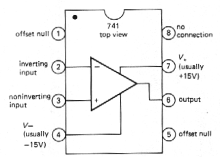 |
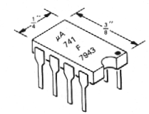
| Fig. 3-1. Universal symbol | Fig. 3-2 . Mini-DIP integrated circuit. | Fig. 3-3. |
The most common op-amp is the mA741 C, or just 741 for
short. It is a wee beastie packaged in the so-called mini-DIP (dual
in-line package), and it looks as shown in Figure 3.2. Inside is a
piece of silicon containing 20 transistors and 11 resistors. The pin
connections are shown in Figure 3.3. The dot in the corner, or notch at
the end of the package, identifies the end from which to begin counting
the pin numbers. As with most electronic packages, you count pins
counterclockwise, viewing from the top. The "offset null" terminals
have to do with correcting (externally) the small asymmetries that are
unavoidable when making the op-amp.
Here are the simple rules for working out op-amp behavior with external feedback. They're good enough for almost everything you'll ever do.
- First, the op-amp voltage gain is so high that a fraction of a millivolt between the input terminals will swing the output over its full range, so we ignore that small voltage => The output attempts to do whatever is necessary to make the voltage difference between the inputs zero.
- Second, op-amps draw very little input current (0.08~A for the 741; picoamps for FET-input types); we round this off => The inputs draw no current.
 |
.
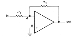
Figure 3-4 |
![]()
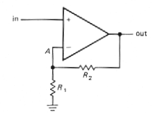
3.04 Inverting amplifier
Let's begin with the circuit shown in Figure 3-4. The analysis is simple, if you remember your golden rules:
- Point B is at ground, so rule 1 implies that point A is also.
- This means that (a) the voltage across R2 is Vout, and (b) The voltage across R1, is Vin,
- So, using rule 2I, we have
in other words, voltage gain = Vout/Vin = - R2/R1.
Later you will see that it's often better not to ground B directly, but through a resistor. However, don't worry about that now.
To understand how feedback works, just imagine some input level, say + 1 volt. For concreteness, imagine that R1, is 10k and R2 is 100k. Now, suppose the output decides to be uncooperative, and sits at zero volts. What happens? R1 andR2form a voltage divider, holding the inverting input at +0.91 volt. The op-amp sees an enormous input unbalance, forcing the output to go negative. This action continues until the output is at the required - 10.0 volts, at which point both op-amp inputs are at the same voltage, namely ground. Similarly, any tendency for the output to go more negative than - 10.0 volts will pull the inverting input below ground, forcing the output voltage to rise.
What is the input impedance? Simple. Point A is always at zero volts (it's called a virtualground). So Zin = R1,. At this point you don't yet know how to figure the output impedance; for this circuit, it's a fraction of an ohm.
Note that this analysis is true even for dc - it's a dc amplifier. So if you have a signal source offset from ground (collector of a previous stage, for instance), you may want to use a coupling capacitor (sometimes called a blocking capacitor, since it blocks dc but couples the signal). For reasons you will see later (having to do with departures of op-amp behavior from the ideal), it is usually a good idea to use a blocking capacitor if you're only interested in ac signals anyway.
This circuit is known as an inverting
amplifier. Its one undesirable feature is the low input
impedance, particularly for amplifiers with large (closed-loop) voltage
gain, where R1, tends to be rather small. That is remedied
in the next circuit (Fig. 3-5).
 |
.
Figure 3-5 |
Consider Figure 3.5. Again, the analysis is
simplicity itself:
VA = Vin
But VA comes from a voltage divider:
VA = VoutR1/(R1
+ R2)
Set VA = Vin, and you get
gain = Vout/ Vin = 1 + R2/R1
This is a noninverting amplifier.In
the approximation we are using, the input impedance is infinite (with a
741 it would be hundreds of megohms, at least; a FET opamp might have Zin
~ 1012W
or more). The output impedance is still a fraction of an ohm. As with
the inverting amplifier, a detailed look at the voltages at the inputs
will persuade you that it works as advertized.
 |
.
Figure 3-6 |
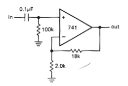
Once again we have a dc amplifier. If the
signal source is ac-coupled, you must provide a return to ground for
the (very small) input current, as in Figure 3-6. The component values
shown give a voltage gain of 10 and a low-frequency 3dB point of 16Hz.
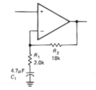
ac Amplifier
Again, if only ac signals are being
amplified, it is often a good idea to "roll off" the gain to unity at
dc, especially if the amplifier has large voltage gain, in order to
reduce the effects of finite "input offset voltage." The circuit in
Figure 3.7 has a low-frequency 3dB point of 17Hz, the frequency at
which the impedance of the capacitor equals 2kW. Note the large capacitor value required. For
noninverting amplifiers with high gain, the capacitor in this ac
amplifier configuration may be undesirably large. In that case it may
be preferable to omit the capacitor and trim the offset voltage to
zero, as we will discuss later (Section 3.12).
An alternative is to raise R1 and R2 perhaps
using a T network for the latter (Section 3.18).
 |
.
Figure 3-7 |
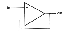
Figure 3.8 shows the op-amp version of an emitter follower. It is simply a noninverting amplifier with R1 infinite and R2 zero (gain = 1). There are special op-amps, usable only as followers, with improved characteristics (mainly higher speed), e.g., the LM310.
An amplifier of unity gain is sometimes
called a bufferbecause of its isolating properties (high
input impedance, low output impedance).
 |
. Figure 3-8 |
3.08 Basic cautions for
op-amp circuits
-
In all op-amp circuits golden rules 1 and 2 (Section 3.03) will be obeyed only if the op-amp is
in the active region, i.e., inputs and outputs not saturated at one of
the supply voltages.
For instance, overdriving one of the amplifier configurations will cause output clipping at output swings near Vccor Vee. During clipping the inputs will no longer be maintained at the same voltage. The op-amp output cannot swing beyond the supply voltages (typically it can swing only to within 2V of the supplies). Likewise, the output compliance of an op-amp current source is set by the same limitation.
- The feedback must be arranged so that it is negative. This means (among other things) that you must not mix up the inverting and noninverting inputs.
- There must always be feedback at dc in an op-amp circuit. Otherwise the op-amp is guaranteed to go into saturation.
For instance , we werw able to put a capacitor from the feeddback network to ground in the noninverting amplifier (to reduce gain at dc to 1), but we could not similarly put a capacitor in series between the output and the inverting input.
- Many op-amps have a relatively small maximum differential input voltage limit. The maximum voltage difference between the inverting and noninverting inputs might be limited to as little as 5 volts in either polarity. Breaking this rule will cause large input currents to flow, with degradation or destruction of the op-amp.
AN OP-AMP SMORGASBORD
In the following examples we will skip the detailed analysis, leaving that fun for you, the reader.
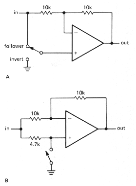
Optional inverter
The circuits in Figure 3.13 let you
invert, or amplify without inversion, by flipping a switch. The voltage
gain is either + 1 or - 1, depending on the switch position.
 |
.
Figure 3-13 |
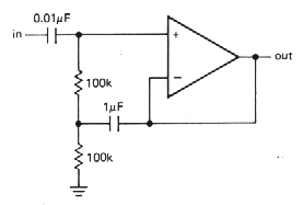
Follower with bootstrap
As with transistor amplifiers, the bias
path can compromise the high input impedance you would otherwise get
with an op-amp, particularly with ac-coupled inputs, where a resistor
to ground is mandatory. If that is a problem, the bootstrap circuit
shown in Figure 3.14 is a possible solution. As in the transistor
bootstrap circuit, the 1mF capacitor makes the upper 100k resistor look like a
high-impedance current source to input signals. The low-frequency
rolloíf for this circuit will begin at about 10Hz, and the response
will drop at 12dB per octave tor frequencies somewhat below this, where
both capacitors contribute to the rolloff.
 |
.
Figure 3-14 |
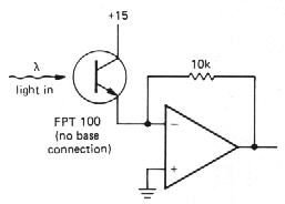
Ideal current-to-voltage converter
Remember that the humble resistor is the
simplest l-to-V converter. However, it has the disadvantage of
presenting a nonzero impedance to the source of input current; this can
be fatal if the device providing the input current has very little
compliance or does not produce a constant current as the output voltage
changes. A good example is a photovoltaic cell, a fancy name
for a sun battery. Even the garden-variety signal diodes you use in
circuits have a small photovoltaic effect (there are amusing stories of
bizarre circuit behavior finally traced to this efifect). Figure 3.15
shows the good way to convert current to voltage while holding the
input strictly at ground. The inverting input is a virtual ground; this
is fortunate, since a photovoltaic diode can generate only a few tenths
of a volt. This particular circuit has an output of 1 volt per microamp
of input current. The resistor from the noninverting input to ground
could be omitted, but it is highly desirable; its function will be
explained shortly in connection with op-amp shortcomings.
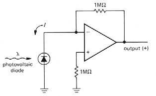 Figure 3-15 |
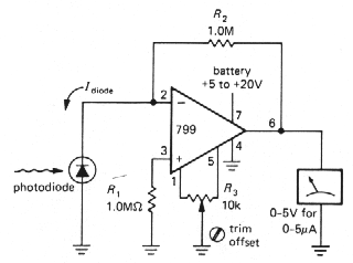 |
Of course, this transresistance configuration
can be used equally well for devices that source their current via some
positive excitation voltage, such as Vcc. Photomultiplier
tubes and phototransistors (both devices that source current from a
positive supply when exposed to light) are often used this way (Fig.
3.16).
 |
.
Figure 3-16 |
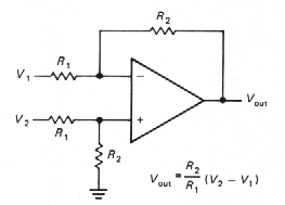
Differential amplifier
The circuit in Figure 3.17 is a
differential amplifier with gain R2/R1,. As
with the current source that used matched resistor ratios, this circuit
requires precise resistor matching to achieve high common-mode
rejection ratios. The best procedure is to stock up on a bunch of 100k
0.01% resistors next time you have a chance. All your differential
amplifiers will have unity gain, but that's easily remedied with
further (single-ended) stages of gain.
 |
.
Figure 3-17 |
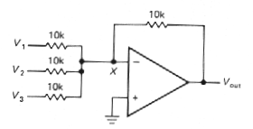
Summing amplifier
The circuit shown in Figure 3.18 is just
a variation of the inverting amplifier. Point X is a virtual ground, so
the input current is V1/R + V2/R + V3/R.That
gives Vout = - (V1 + V2 + V3).
Note that the inputs can be positive or negative. Also, the input
resistors need not be equal; if they're unequal, you get a weighted
sum. For instance, you could have four inputs, each of which is + 1
volt or zero, representing binary values 1, 2, 4, and 8. By using input
resistors of 10k, 5k, 2,5k, and 1,25k you will get an output in volts
equal to the binary count input. This scheme can be easily expanded to
several digits. It is the basis of digital-to-analog conversion,
although a different input circuit (an R-2R ladder) is usually
used.
 |
.
Figure 3-18 |
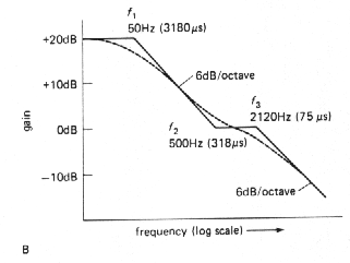
RIAA preamp
The RIAA preamp is an example of an
amplifier with a specifically tailored frequency response. Phonograph
records are cut with approximately flat amplitude characteristics;
magnetic pickups, on the other hand, respond to velocity, so a playback
amplifier with rising bass response is required. The circuit shown in
Figure 3.19 produces the required response. The RIAA playback amplifier
frequency response (relative to 0dB at 1 kHz) is shown in the graph,
with the breakpoints given in terms of time constants. The 47mF capacitor to ground rolls
off the gain to unity at dc, where it would otherwise be about 1000; as
we have hinted earlier, the reason is to avoid amplification of dc
input "offsets". The 739 is a low-noise dual op-amp intended for audio
applications.
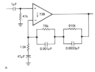 |
. Figure 3-19 Op-amp RIAA phono playback amplifier.
|
 |
Op-amps allow you to make
nearly perfect integrators, without the restriction that Vout<<Vin.
Figure 3.43 shows how it's done. Input current Vin / R flows
through C. Since the inverting input is a virtual ground, the output
voltage is given by
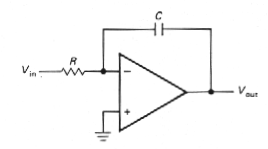 |
<--Figure
3-43 |
The input can, of course, be a
current, in which case R will be omitted. One problem with this circuit
as drawn is that the output tends to wander off, even with the input
grounded, due to op-amp offsets and bias current. This problem can be
minimized by using an FET op-amp for low input current and offset,
trimming the op-amp input offset voltage, and using large R and C
values. In addition, in many applications the integrator is zeroed
periodically by closing a switch placed across the capacitor (usually
an FET), so only the drift over short time scales matters. As an
example, an inexpensive FET op-amp like the LF355 (30pA bias current)
trimmed to a voltage offset of 0.2mV and used in an integrator with R =
10MW and
C = 10mF
will produce an output drift of less than 0.003 volt in 1000 seconds.
 |
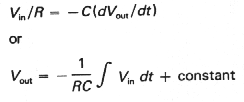
| Figure 3-44 Op-amp integrators with reset switches |
If the residual drift of the
integrator is stil too large for a given application, it may be
necessary to put a large resistor R2 across C to provide dc
feedback for stable biasing. The effect is to roll off the integrator
action at very low frequencies, f < 1 /R2C. Figure
3.44 shows integrators with FET zeroing switch and with resistor bias
stabilization.
 |
.
Figure 3-45 |
The feedback resistor may
become rather large in this sort of application. Figure 3.45 shows a
trick for producing the effect of a large feedback resistor using
smaller values. In this case the feedback network behaves like a single
10MW
resistor in the standard inverting amplifier circuit giving a voltage
gain of - 100. This technique has the advantage of using resistors of
convenient values without the problems of stray capacitance, etc., that
occur with very large resistor values.
F - Použitie integrátora v jadrovej elektronike - nábojový zosilňovač
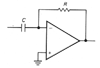
Differentiators are similar to
integrators, but with R and C reversed (Fig. 3.46). Since the inverting
input is at ground, the rate of change of input voltage produces a
current / = C(dVin / dt) and hence an output voltage
Figure 3-46 -> |
 |
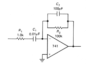
Differentiators are
bias-stable, but they generally have problems with noise and
instabilities at high frequencies because of the op-amp's high gain and
internal phase shifts. For this reason it is necessary to roll off the
differentiator action at some maximum frequency. The usual method is
shown in Figure 3.47. The choice of the rolloff components R1
and C2 depends on the noise level of the signal and the
bandwidth of the op-amp. At high frequencies this circuit becomes an
integrator, due to R1 and C2.
 |
.
Figure 3-47 |
|
|