 |
FEEDBACK
AND OPERATIONAL AMPLIFIERS
(Some selected section from CHAPTER
3 of the book "The Art of Electronics", written by Paul Horowitz and Winfield
Hill, Cambridge University Press , 1985.)
|
|
|
|
|
|
BASIC OP-AMP CIRCUITS |
|
|
COMPARATORS AND SCHMITT TRIGGER |
|
|
FEEDBACK WITH AMPLIFIERS |
|
|
FEEDBACK AMPLIFIER FREQUENCY COMPENSATION |
![]()
3.11 Departures from ideal op-amp
performance
The ideal op-amp has these characteristics:
- Input impedance (differential or common mode) = infinity
- Output impedance (open loop) = 0
- Voltage gain = infinity
- Common-mode voltage gain = 0
- Vout= 0 when both inputs are at the same voltage (zero "offset voltage")
- Output can change instantaneously (infinite slew rate)
Real op-amps depart from these characteristics
in the following ways.
Input current
The input terminals sink (or source, depending on the op-amp type) a small current called the input bias current, IB, which is defined as half the sum of the input currents with the inputs tied together (the two input currents are approximately equal and are simply the base currents of the input transistors). For the 741 the bias current is typically 80nA (0.08mA). The significance of input bias current is that it causes a voltage drop across the resistors of the feedback network, bias network, or source impedance.
Op-amps are available with input bias currents
down to a nanoamp or less for (bipolar) transistor-input circuit types
or down to a few picoamps (10-6mA)
for FET input circuit types. The very lowest bias currents are typified
by the superbeta Darlington LM 11, with an input current of 25pA, and the
MOSFET ICH8500, with an input current of 0.01 pA. In general, transistor
op-amps intended for high-speed operation have higher bias currents.
Input offset current
Input offset current is a fancy name for
the , difference in input currents between the two inputs. Unlike input
bias current, the offset current, los, is a result of manufacturing
variations, since an op-amp"s symmetrical input circuit would otherwise
result in identical bias currents at the two inputs. The significance is
that even when it is driven by identical source impedances the op-amp will
see unequal voltage drops and hence a difference voltage between its inputs.
Typically, the offset current is about onetenth the bias current. For the
741, Ioffset = 10nA, typical.
l Input impedance
Input impedance refers to the differential
input resistance (impedance looking into one input, with the other input
grounded), which is usually much less than the common-mode resistance (a
typical input stage looks like a long-tailed pair with current source).
For the 741 it is about 2MW.
FET-input op-amps typically have Rin~ 1012 ohms or
more. Because of the input bootstrapping effect of negative feedback (it
attempts to keep both inputs at the same voltage, thus eliminating most
of the differential input signal), Zin in practice is raised
to very high values and usually is not as important a parameter as input
bias current.
Common-mode input range
The inputs to an op-amp must stay within
certain voltage range, typically less than the full supply range, for proper
operation. If the inputs go beyond this range, the gain of the op-amp may
change drastically, even reversing sign! For a 741 operating from ± 15
volt supplies, the common-mode input range is ± 12 volts. There are op-amps
available with common-mode input ranges down to the negative supply (e.g.,
the LM358, a dual op-amp in mini-DIP package, or the 3130/3140 series)
and up to the positive supply (the 301 /307, or the 355-357 series, for
instance). In addition, there are maximum allowable input voltages beyond
which damage will result. For the 741, they are ± 15 volts or the supply
voltages, whichever are less.
Dífferential input range
Some op-amps allow only a limited voltage
between the inputs, sometimes as small as ±0.5 volt, although most are
more forgiving, permitting differential inputs nearly as large as the supply
voltages. Exceeding the specified maximum can degrade or destroy the op-amp.
l Output impedance; output swing versus load resistance
Output impedance Ro means
the op-amp's intrinsic output impedance without feedback. For the
741 it is about 75 ohms, but with some low-power op-amps it can be as high
as several thousand ohms. Feedback lowers the output impedance into insignificance
(or raises it, for a current source); so what usually matters more is the
maximum output current, with typical values of 20mA or so. This is frequently
given as a graph of output voltage swing Vom as a function
of load resistance, or sometimes just a few values for typical load resistances.
For the ubiquitous 741, output swings to within about 2 volts of VCC
and
VEE are possible into load resistances greater than
about 2k. Load resistances significantly less than that will permit only
a small swing. Some op-amps can produce output swings all the way down
to the negative supply (e.g., the LM358), a particularly ` useful feature
for circuits operated from a single positive supply, since output swings
all the way to ground are then possible. Finally, op-amps with MOS transistor
outputs (e.g., the CA3130 and CA3160) can swing all the way to both supply
rails.
l Voltage gain and phase shift
Typically the voltage gain Avo
at dc is 100,000 to 1,000,000 (often specified in' decibels), dropping
to unity gain at a frequency (called fT) of 1 MHz to
10MHz. This is usually given as a graph of open-loop voltage gain as a
function of frequency. For internally compensated op-amps this graph
is simply a 6dB/octave rolloff beginning at some fairly low frequency (for
the 741 it begins at about 100Hz), an intentional characteristic necessary
for stability, as you will see in Section
3.31. This rolloff (the same as a simple RC low-pass
filter) results in a constant 90° lagging phase shift from input to output
(open-loop) at all frequencies above the beginning of the rolloff, increasing
to 120 ° to 160 ° as the open-loop gain approaches unity. Since a 180°
phase shift at a frequency where the voltage gain equals 1 will result
in positive feedback (oscillations), the term "phase margin" is used to
specify the difference between the phase ' shift at fT and 180
° .
Input offset voltage
Op-amps don't have perfectly balanced input stages, owing to manufacturing variations. If you connect the two inputs together for zero input signal, the output will usually saturate at either VCCor VEE(you can't predict which). The difference in input voltages necessary to bring the output to zero is called the input offset voltage Vos (it's as if there were a battery of that voltage in series with one of the inputs). Usually op-amps make provision for trimming the input offset vottage to zero. For a 741 you use a 10k pot between pins 1 and 5, with the wiper connected to VEE.
Of greater importance for precision applications
is the drift of the input offset voltage with temperature and time, since
any initial offset can be trimmed to zero. A 741 has a typical offset voltage
of 2mV (6mV maximum) and unspecified coefficients of offset drift with
temperature and time. The OP-07, a precision op-amp, is laser-trimmed for
a typical offset of 30 microvolts, with temperature coefficient
TCVosof
0.2mV/°C and long-term drift of 0.2mV/month.
Slew rate
The op-amp "compensation" capacitance and small internal drive currents act together to limit the rate at which the output can change, even when a large input unbalance occurs. This limiting speed is usually specified as slew rate or slewing rate (SR). For the 741 it is 0.5V/ms; a high-speed op-amp might slew at 100V/ms, and the LH0063C "damn fast buffer" slews at 6000V/ms. The slew rate limits the amplitude of a sine-wave output swing above some critical frequency (the frequency at which the full supply swing requires the maximum slew rate of the opamp), thus explaining the "output voltage swing as a function of frequency" graph. A sine wave of frequency f hertz and amplitude A volts requires a minimum slew rate of 2pAf volts per second.
For externally compensated op-amps the
slew rate depends on the compensation network used. In general, it will
be lowest for "unity gain compensation," increasing to perhaps 30 times
faster for x 100 gain compensation. This is discussed further in Section
3.31.
Temperature dependence
All these parameters have some temperature dependence. However, this usually doesn't make any difference, since small variations in gain, for example, are almost entirely compensated by feedback. Furthermore, the variations of these parameters with temperature are typically small compared with the variations from unit to unit.
The exceptions are input offset voltage and input offset current. This will matter, particularly if you've trimmed the offsets approximately to zero, and will appear as drifts in the output. When high precision is important, a low-drift "instrumentation" opamp should be used, with external loads kept above 10k to minimize the horrendous effects on input-stage performance caused by temperature gradients.
For completeness, we should mention here
that op-amps are also limited in common-mode rejection ratio (CMRR), power-supply
rejection ratio (PSRR), input noise voltage and current (en
, in) and output crossover distortion. These become
significant limitations only in connection with precision circuits and
low-noise amplifiers.
3.12 Effects of op-amp
limitation on circuit behavior
Let's go back and look at the inverting
amplifier with these limitations in mind. You will see how they affect
performance, and you will learn how to design effectively in spite of them.
With the understanding you will get from this example, you should be able
to handle other op-amp circuits. Figure 3.28 shows the circuit again.
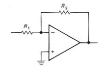 |
Figure 3-28 |
Open-loop gain
Because of finite open-loop gain, the voltage
gain of the amplifier with feedback (closedloop gain) will begin dropping
at a frequency where the open-loop gain approaches R2/R1
(Fig.
3.29). For garden-variety op-amps like the 741, this means that you're
dealing with a relatively low frequency amplifier; the open-loop gain is
down to 1000 at 1 kHz, and fT is 1MHz. Note that the
closed-loop gain is always less than the open-loop gain; this means, for
instance, that a x 1000 amplifier built with a 741 will show a noticeable
falloff of gain for frequencies approaching 1kHz. Later in the chapter
(Section 3.24),
when we deal with transistor feedback circuits with finite open-loop gains,
we will have a more accurate statement of this behavior.
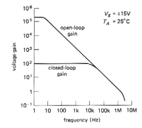 |
Figure 3-29 |
Slew rate
Because of limited slew rate, the maximum
sine-wave output swing drops above a certain frequency. Figure 3.30 shows
the curve for a 741, with its 0.5V/ms
slew rate. For slew rate S, the output amplitude is limited to A (pp)
<= S/pf
for a sine wave of frequency f, thus explaining the 1/f dropoff
of the curve. The flat portion of the curve reflects the power-supply limits
of output voltage swing.
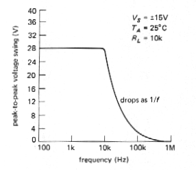 |
Figure 3-30 |
Output current
Because of limited output current capability,
an op-amp's output swing is reduced for small load resistances. Figure
3.31 shows the graph for a 741. For precision applications it is a good
idea to avoid large output currents in order to prevent on-chip thermal
gradients produced by excessive power dissipation in the output stage.
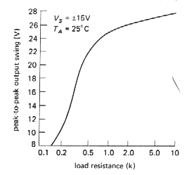 |
Figure 3-31 |
Offset voltage
Because of input offset voltage, a zero input produces an output of Vout=GdcVos. For an inverting amplifier with voltage gain of 100 built with a 741, the output could be as large as ±0.6 volt when the input is grounded (Vos = 6mV max). Solutions:
- If you don"t need gain at dc, use a capacitor to drop the gain to unity at dc, as in the RIAA amplifier circuit earlier. In this case you could do that by capacitively coupling the input signal.
- Trim the voltage offset to zero using the manufacturer's recommended trimming network.
- Use an op-amp with smaller Vos.
Because of finite input current, zero input
voltage still won't give zero output, even if the input offset voltage
is trimmed to zero. The inverting input terminal sees a driving impedance
of R1||R2, so the bias current produces a voltage
Vin
= IB(R1|| R2), which is then amplified
by the gain at dc, -R2/R1.
For a 741 connected
with R1= 100k and R2=1MW,
the output (for grounded input) could be as large as 10 x 200nA x 91 k,
or 0.18 voIt (GdcIBRunbalance; IB
=200nA max).
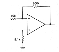 |
Figure 3-32 |
To minimize the effects of input bias current,
it is a good idea to ensure that both inputs see the same dc driving resistance,
as in Figure 3.32. In this case, 9.1k is chosen as the parallel resistance
of 10k and 100k. In addition, it is best to keep the resistance of the
feedback network small enough so that bias current doesn't produce large
offsets; typical values for the resistance seen from the op-amp inputs
are 1k to 100k or so. A third cure involves dropping the gain to unity
at dc, as before. If you're still in trouble with errors produced by bias
current, use an op-amp with lower bias current. The inexpensive LM308 has
IB=1.5nA
(typ), its improved cousin (the LM 11) has IB=25pA (typ),
the popular LF355-LF357 seriés of FET-input op-amps has IB=30pA,
and the recent CA3140 and CA080 series, priced at under a dollar, have
IB
= 10pA (typ).
Input offset current
Because of input offset current, even a
circuit with balanced input impedances at dc will suffer some output offset.
This differential effect is usually quite a bit smaller than the output
offset produced by input bias current with unbalanced input resistances,
so it is worth balancing the input resistances. If the remaining output
offset is too large for a given application, the only solution (besides
lower resistances in the feed back network) is a lower input current opamp.
Limitations imply tradeoffs
The limitations of op-amp performance we have talked about will have an influence on component values in nearly all circuits. For instance, the feedback resistors must be large enough so that they don't load the output significantly, but they must not be so large that input bias current produces sizable offsets. High impedances in the feedback network also increase susceptibility to capacitive pickup of interfering signals and increase the loading effects of stray capacitance. These tradeoffs typically dictate resistor values of 2k to 100k with generalpurpose op-amps like the 741.
Similar sorts of tradeoffs are involved
in almost all electronic design, including the simplest circuits constructed
with transistors. For instance, the choice of quiescent current in a transistor
amplifier is limited at the high end by device dissipation, increased input
current, excessive supply current, and reduced current gain, whereas the
lower limit of operating current is limited by leakage current, reduced
current gain, and reduced speed (from stray capacitance in combination
with the high resistance values). For these reasons you typically wind
up with collector currents in the range of a few tens of microamps to a
few tens of milliamps (higher for power circuits, sometimes a bit lower
in "micropower" applications).
|
|