 |
Pulse
processing and Analyses
Dušan
Kollár, |
|
|
|
|
|
Amplitude (Pulse Height) Measurements |
|
|
Frequency and time response of amplifiers |
|
|
Detector equivalent circuits |
|
|
Nuclear detector analog signal processing |
|
|
ADC - digitization of pulse high |
|
|
Timing measurement |
|
|
Time interval measurement |
![]()
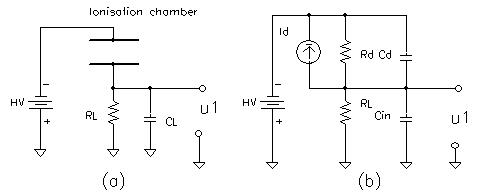
| Detector equivalent circuit |
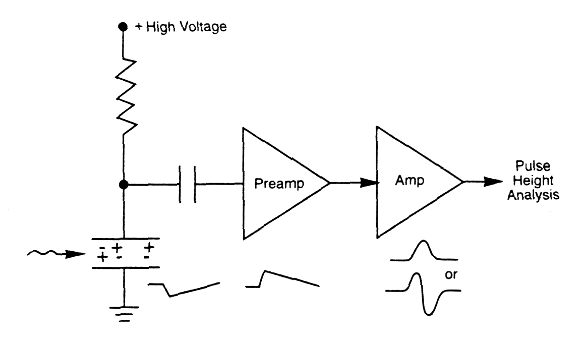 |
Fig. m-9 Basic Detector and
Amplification Stages |
By applying detector bias an electric field is created, which causes the charge carriers to migrate and be collected. During the charge collection a small current flows, and the voltage drop across the bias resistor is the pulse voltage.
From point of distribution of dc voltage across detector and load resistor RL practically whole high dc voltage is laid on detector. Current flowing through the load resistor is practically independent from value of HV power supply -> it is property that specifies the current sources.
Most detectors can be displaced with
equivalent circuit
- model, consisting of pulse current source with yours internal
resistance Rd and capacitor, which figures capacitance Cd
of the detector.
 |
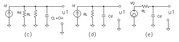 |
| Fig. m-10 Equivalent circuit of detector (e.g. ionization chamber). Detector is represented with his interior parameters (resistance Rd >>RL and capacitance Cd ) and load resistor RL and capacitance CL .Resulting integrating chain capacitance Cd~ Cd+CL+Cin includes input amplifier capacitance Cin too. Resulting detector equivalent circuit in current variant (d) or voltage variant (e). |
In most cases high resistance Rd of reverse-biased junction, or other internal detector resistance effects negligible. Equivalent detector circuits works then with parallel combination Rd and RL => RL||Rd~RL.
Current signal from detector can be delivered to preamplifier directly (dc-coupling) or via isolating capacitor. (For high charge transfer efficiency admittance representing capacitance of coupling capacitor => differentiate capacitance of shaping amplifier.)
Because the maximal output voltage
amplitude from
the detector (Umax= QD/Cd) is
determined
by the capacitance Cd, for the shaping purpose we can use
only
resistance RL in time constant RLCd,
from
which depends acceptable counting rates of detector events (according
to
collection time of charge carriers - ti) .
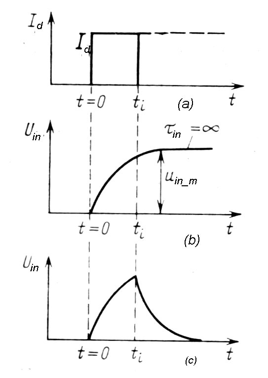 |
Fig.
m-11
Influence of the RLCd input chain on the pulse shape. Let`s suppose:
|
On figure above pulse height is Id and pulse duration ti. If the load resistance RL is very height, e.g RL~iinfinite and so tin=RLCd=infinite, then in time of the pulse duration tiis capacitor Cd charged with full charge Q=Idti=Uin_mCd, and the maximal pulse height Uin_m=Q/Cd can be reached by decreasing the capacitance Cd.
In real detector output circuit
the resistance
RLmust
be pick up in accordance with the time resolution of the detector but
with
minimal drop off pulse amplitude. From the next figure you can see
that,
with given pulse duration ti and detector capacitance Cd,
the determinate drop off pulse height depends on time constant tin,
respectively on resistance RL.
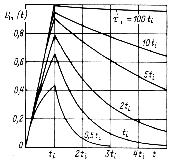 |
Fig. m-12
Dependence pulse height Uin and pulse shape vs. integration time constant tin=RLCd and pulse time duration ti. |
![]()
Option of the input time constant tin=RLCd
Time constant tin=RLCd>> ti (case RL> 100MW) can increase collecting pulse amplitude but makes long decay time constant.
Time constant tin=RLCd<< ti (case RL~ 50-100W) shortens pulse duration (useful for high counting rates) but decreases pulse high.
For most scintillation
spectrometer
is acceptable
| tin=RLCd~ ti. |
 |
| Fig. m-13
Pulse sampled from the pulse ionization chamber in case of:
|
![]()
Impact of the input integration chain
It was already mentioned that for most scintillation spectrometer is acceptable tin=RLCd~ ti, whith some drop off pulse amplitude. For better quality comparing, concept of "ballistic error" D A=Amax-A0 was established.
 |
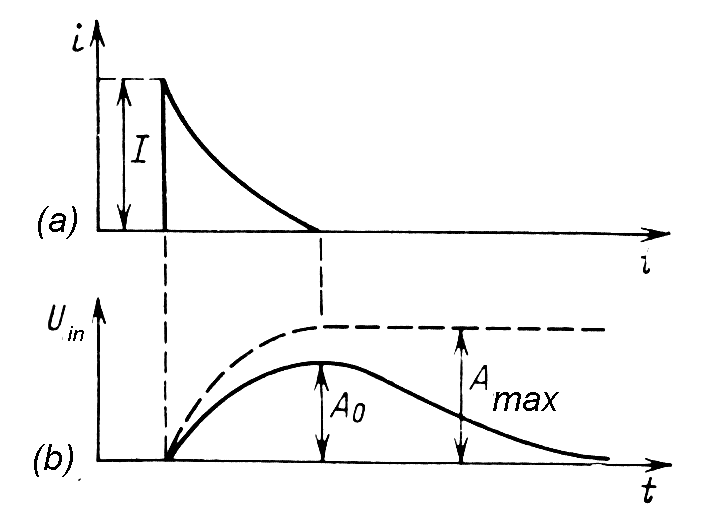
Fig. m-14 |
|
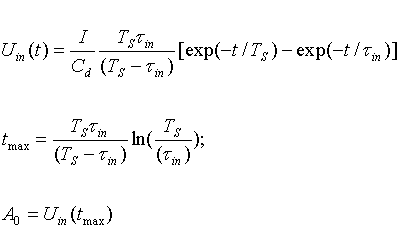
| Scintillation pulse current id=I*exp(-t/TS) in equivalent detector circuit is divided in RL and Cd. After Laplacce transform we obtain |
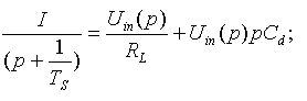 |
| From time-domain response Uin(t) in time tmax we obtain then pulse height A0 on the output of the scintillation detector whit real time constant tin=RLCd<>infinite. |
 |
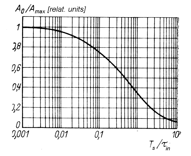 |
Fig.
m-15
llustration of the so called "ballistic error" D A=Amax-A0 vs. ratio TS/tin scintillation time constant TS and input ciruit time constant tin .
|
From this figure you can see that for scintillation spectrometer applications has no reason to make tin= RLCd shorter than 10TS, e.g. in scintillator NaI(Tl) (TS=0,3ms) with Cd~5pF and RL=0,5MW preserves time constant tin=RLCd~3ms.
| Nuclear detector analog signal processing |
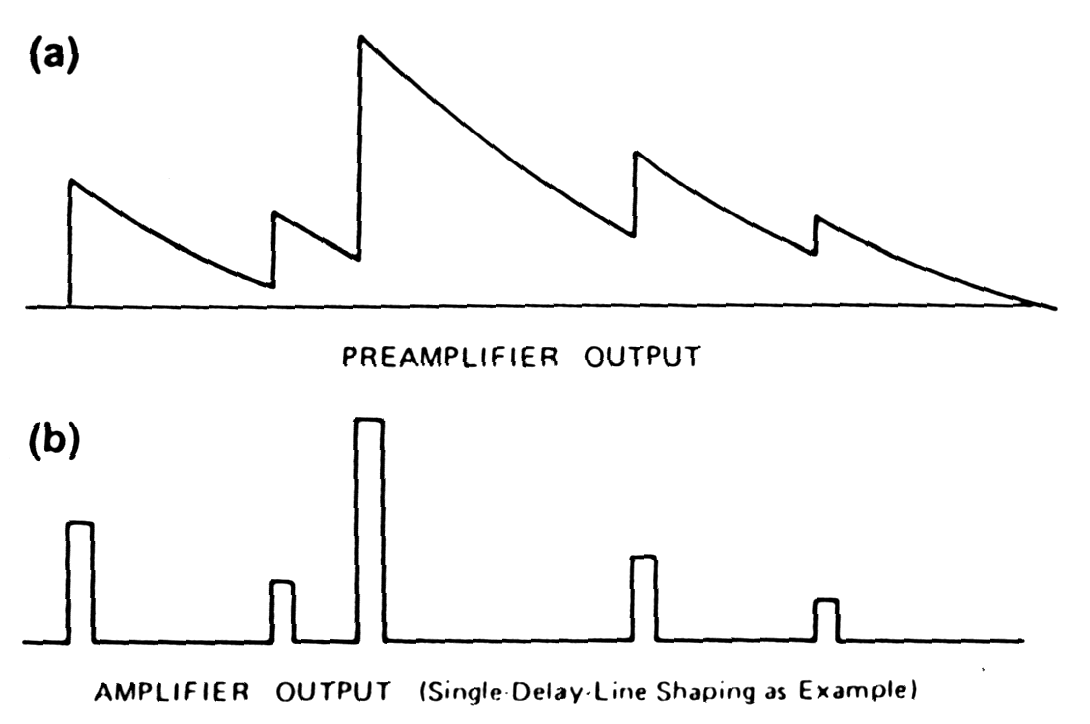 |
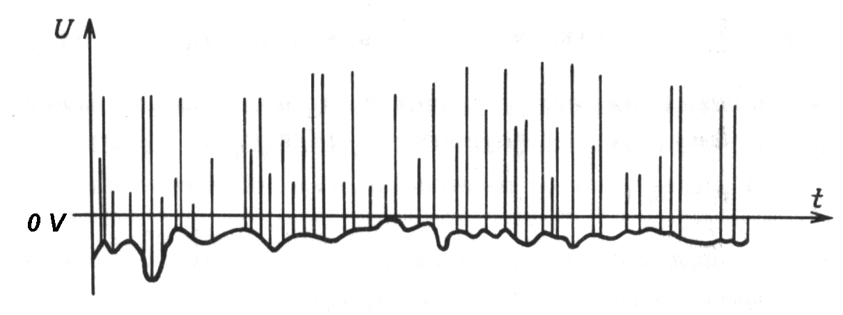
Fig. m-16 Pulses pile-up affect on baseline fluctuations and cause loss of resolution of pulse amplitude measurement:
|
Before amplification, the pulse-shaping amplifier must replace the long decay time of the preamplifier output pulse with a much shorter decay time (with preserving the energy information representing by pulse amplitude). Otherwise the acceptable counting rate would be severely restricted.
Possible ways to short pulse duration:
- CR – RC pulse shaping;
- Pole-zero cancellation shaping;
- Delay-line shaping .
| CR - RC pulse shaping |
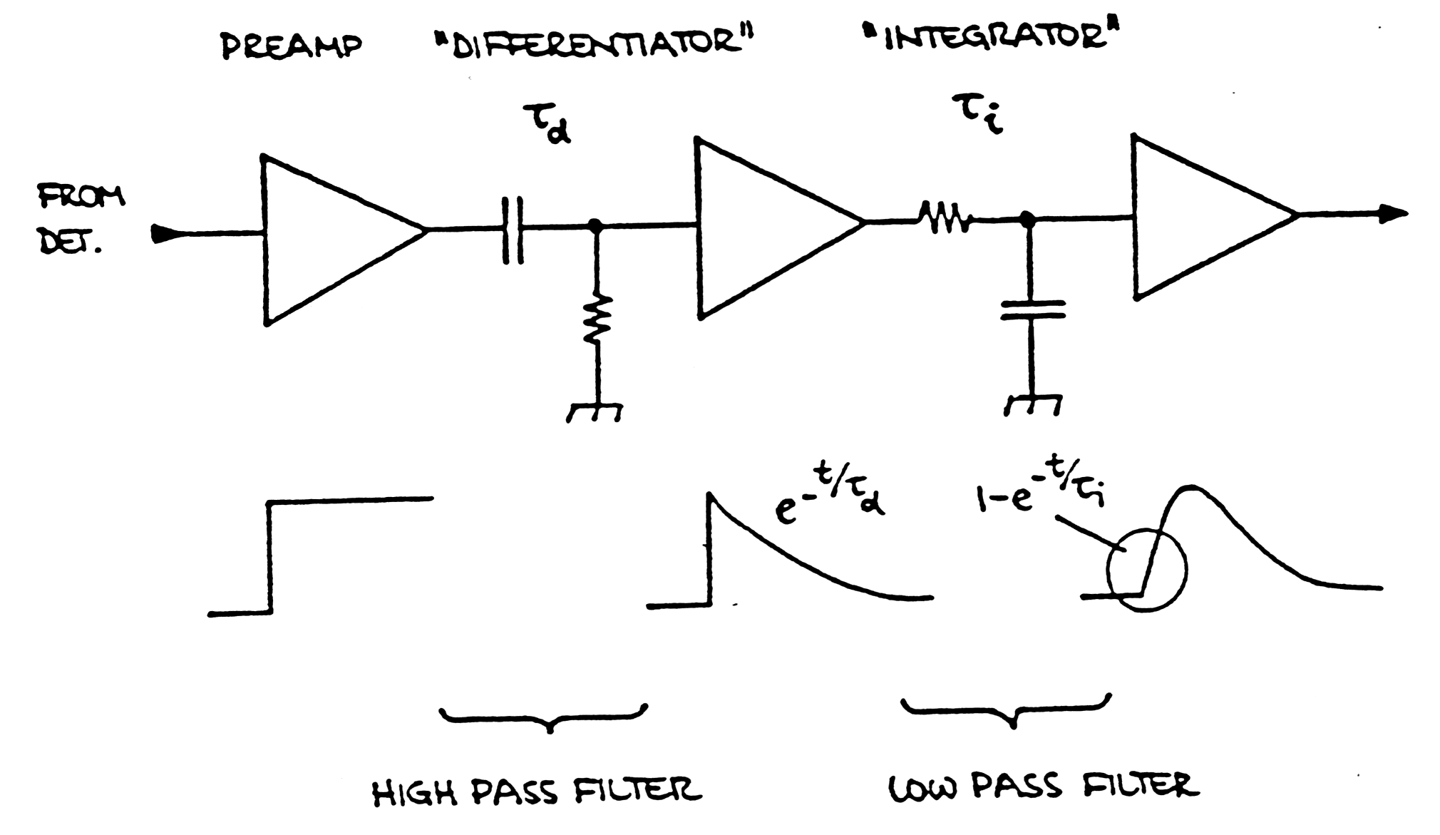 |
Fig. m-17
Equivalent circuit of amplifier:
|
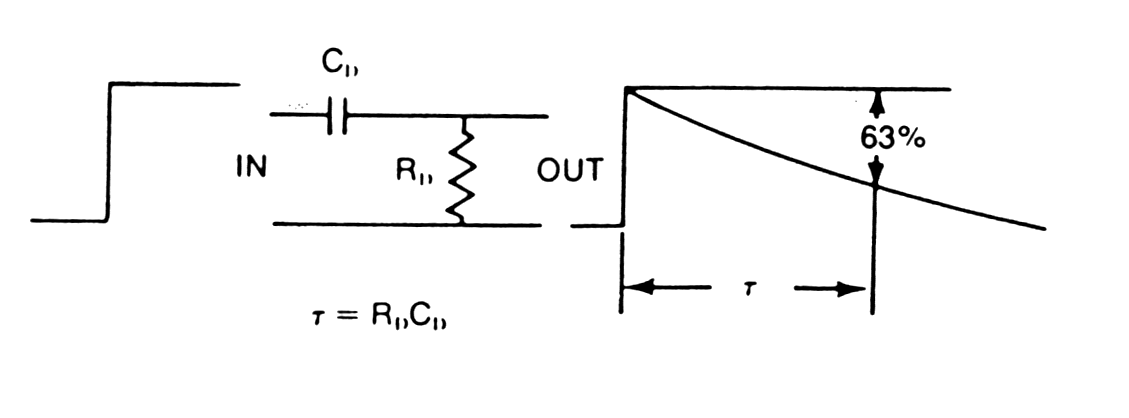 |
Fig. m-18
CR Differentiation - simple tool for pulse shorting. |
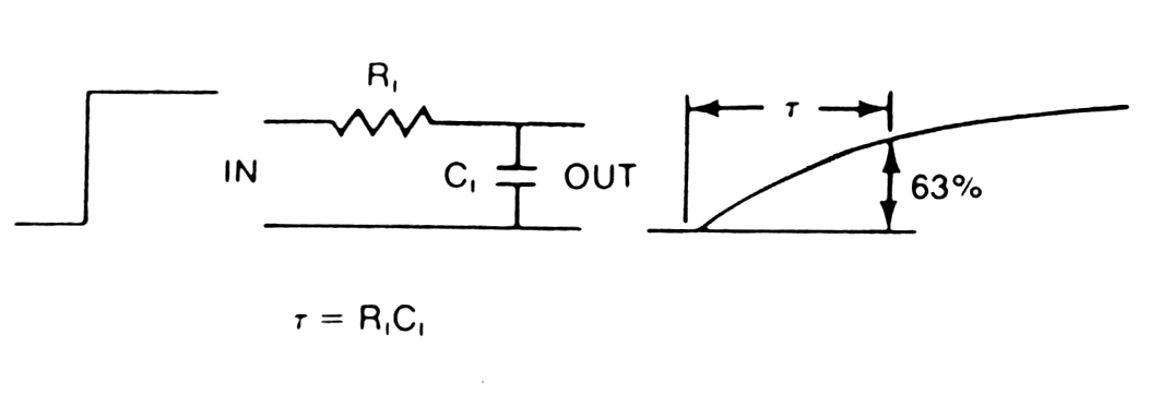 |
Fig.
m-19
RC Integration |
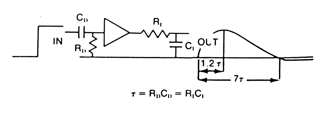 |
Fig.
m-20
CR-RC pulse shaping |
Best pulse shape from point of noise/signal (S/N) consideration is theoretical calculated pulse form in next figure (a).
To improve S/N ratio in amplifiers typically is set shaping time constant:
td~tI=RC
This noise performance (case - e in next fig.) is only 36% worse than optimum filter with the same time constant. The simple arrangement is useful for estimates, since simple to evaluate.
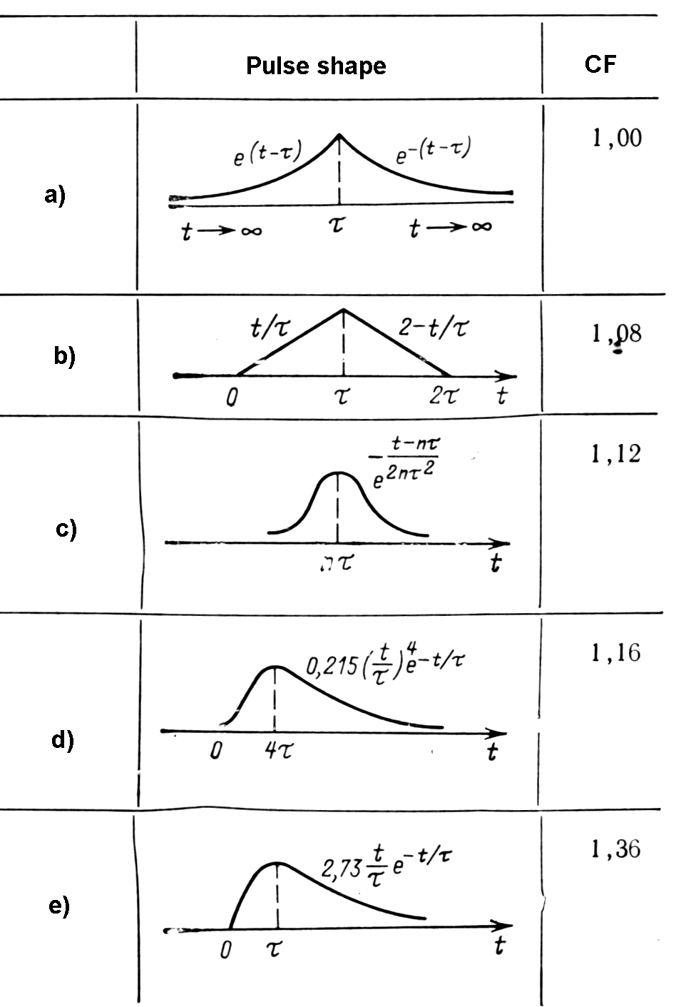 |
Fig.
m-21 Pulse shape for optimal S/N
in amplifiers. Factor CF makes possible to compare the optimal
theoretical
calculated pulse (a) form with real filter pulse shaping.
|
By replacing the
simple RC integrator with more complicated
active network => S/N improved by 17% to 19% at noise corner time
constant.
 |
Fig.
m-22
Semi-Gaussian (CR+RCn) pulse shaping. Increasing number n of RC output pulse shape changes its form to symmetrical pulse. |
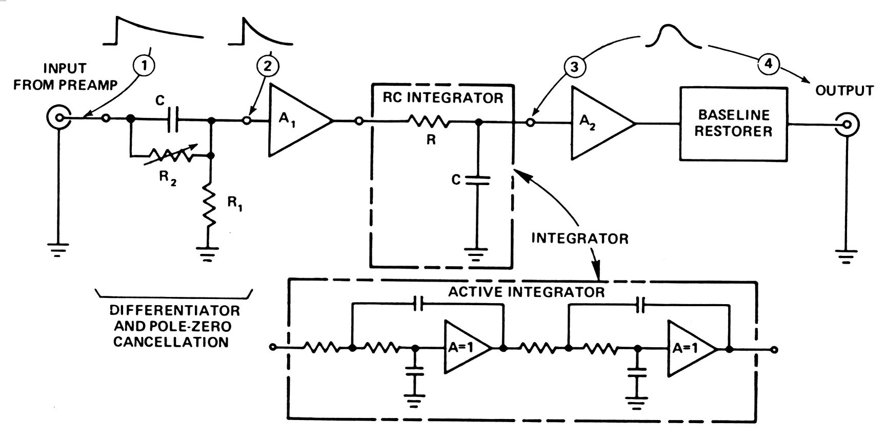 |
Fig.
m-23
Example of so called active filter, based on operation amplifier - modern method pulse shaping in the Semi-Gaussian Shaping Amplifier. |
![]()
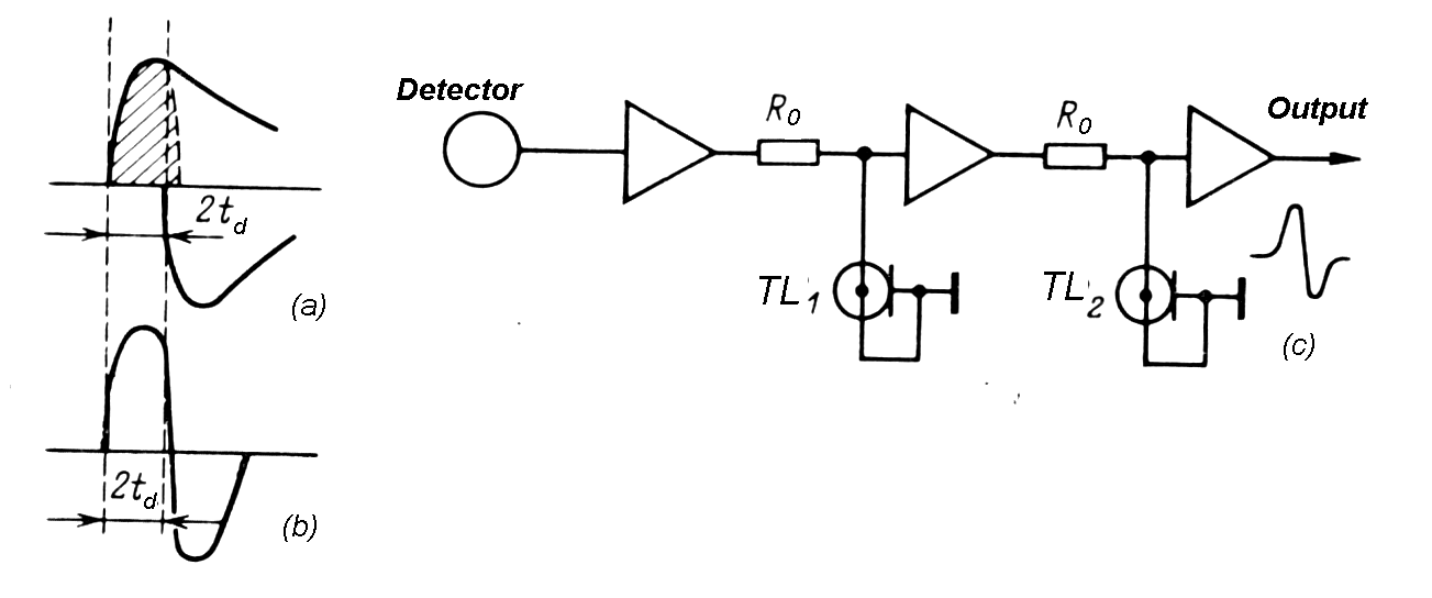
| Delay-line shaping |
Drawback of CR-RC shaping is much longer pulse duration compared with delay-line shaping.
Simple delay line
clipping of scintillator pulses
illustrates next figure. Goal is to short pulses for improved count
rate
capability.
 |
Fig. m-27a
Delay line clip as a shaping circuits. |
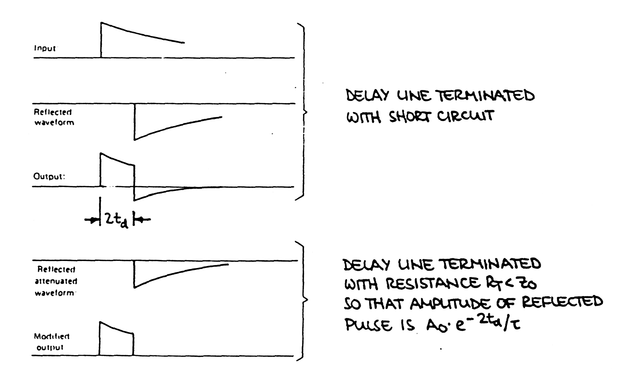 |
Fig. m-27b
Coax line terminated with short circuits allow to use reflected and delayed waveform (inverted pulse) for shaping pulse of duration 2td . |
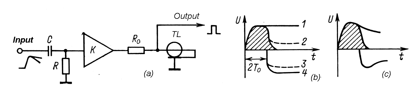 |
Fig.
m-28 Two
stage shortening circuits:
2 – modified output; 3 – attenuted reflected wave; 4 – reflected wave. |
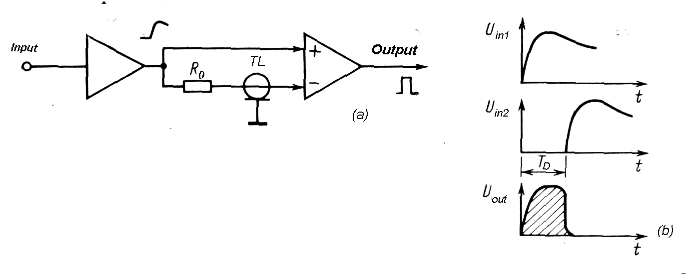 |
| Fig. m-29
Cable delay in one input
path to differential amplifier. Distance unit of line clip makes delay
T0=(LC)0,5
R0=(L/C) 0,5 is
terminating
resistance; |
![]()
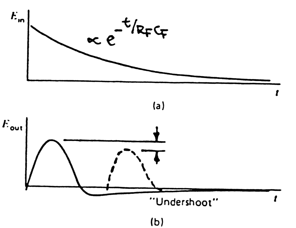
| Pole-zero cancellation (PZC) |
Bipolar output
pulse is obtained when 2 differentiate
chains are inserted. Double CR -differentiate shaping produces a
bipolar
pulse with equal area in its positive/ negative lobes. CR-RC-CR shaping
case to undershoot and loss of resolution due to baseline fluctuations.
At medium to high counting rates a substantial fraction of the
amplitude
pulses will ride on the undershoot from the previous pulse, pulse have
longer duration and worse S/N ratio, what cause broadening of the
energy
peaks.
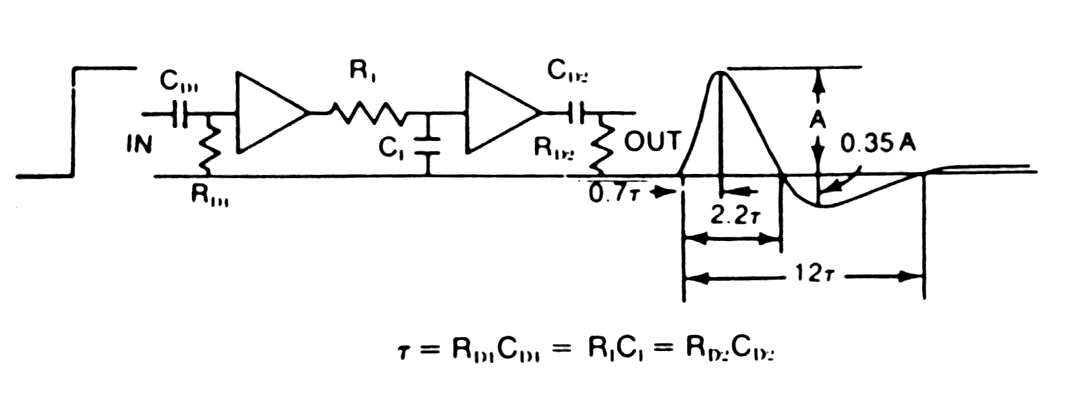 |
Fig. m-25 Doubly-Differentiated CR-RC-CR Shaping - thereason way can an undershoot be generated. | |
Feedback
capacitance in charge sensitive preamp must
be discharged too. Conventionally it is done with resistor. Output is
no
longer a step, but decays exponentially. Exponential decay superimposed
on shaper output. Small amplitude overshoot decays back to baseline,
with
long time constant, provided by the preamplifier output pulse often
occurs.
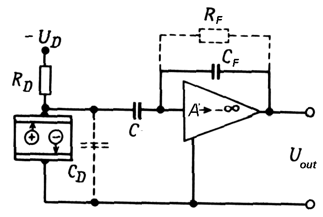 |
Fig. m-26a | |
 |
 |
|
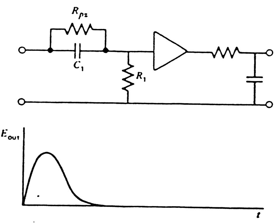
| Issue of pulse undershoot on preamp output | ||
Because
conventional CR-RC shaping case to undershoot
and loss of resolution due to baseline fluctuations in Pole-Zero
Cancellation
(PZC) the resistor Rpzis
added in parallel with capacitor. Resistance Rpz must be
precisely
adjusted for good baseline recovery (=> simple exponential
decay
to baseline) especially at high counting rates.
| The benefit of Pole-Zero cancellation |
 |
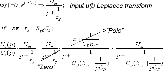 |
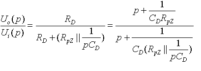
| "Zero"compensates "pole"of the transfer function. |
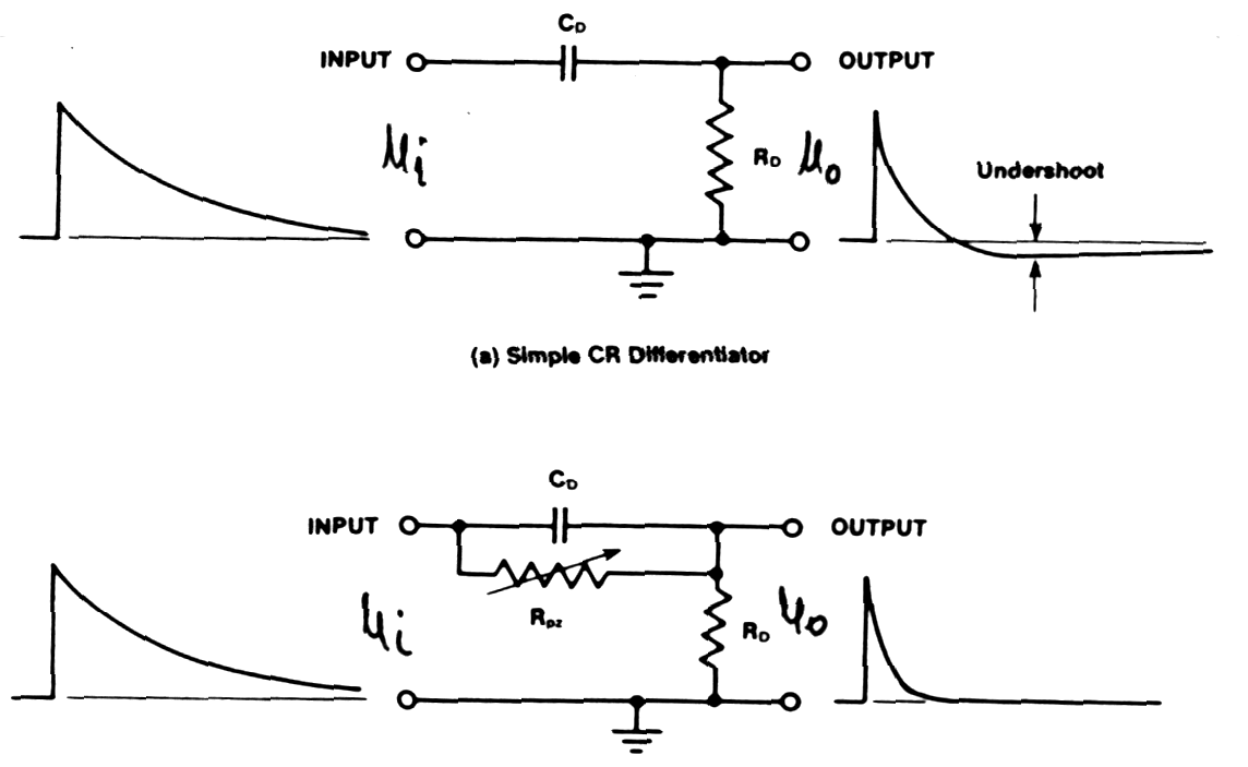 |
Fig. m-26b
=> no undershoot and loss of resolution due to baseline fluctuation. |
![]()
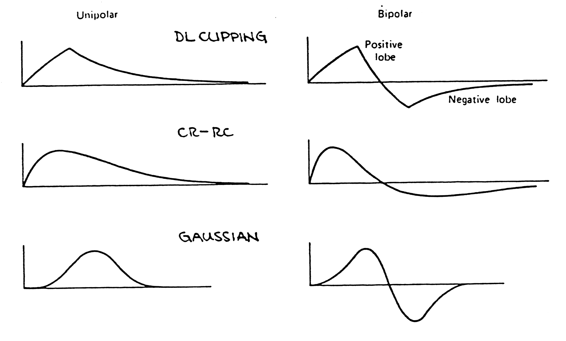
| Unipolar versus bipolar shaping |
The bipolar shape is useful in minimizing baseline shift with varying counting rates when ac-coupling is used. Electronic resolution with bipolar shaping is typically 25-50% worse than for corresponding unipolar shaper. However:
- Bipolar shaping eliminates baseline shift (dc comp.=0), pole zero adjustment is less critical + added suppression of low frequency pick up.
- Not all measurements require optimum noise performance. Bipolar shaping is much more convenient for user (important in larger systems!) Often the method of choice.
 |
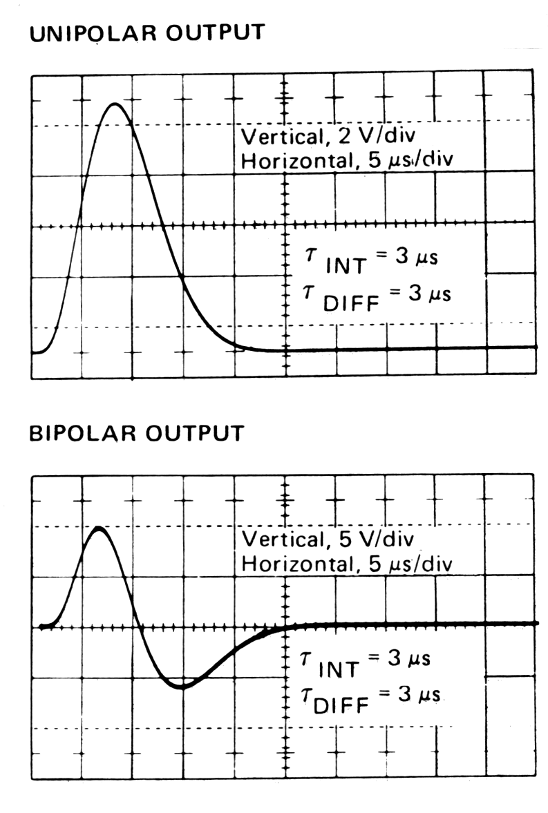 |
| Fig. m-30 Unipolar pulse after second differentiator changes to bipolar pulse. | Typical unipoloar and bipolar output pulse shapes from a semi-Gaussian shaping amplifier. |
 |
| Fig. m-31
Creating bipolar pulse on base of double delay lines, terminated with short circuits (from input side is coax terminated with resistor R0~Z0 and no reflection occurs). Duration of bipolar pulse is 2td ( td - wave propagation time across line) |
![]()
| Base-line restoration (BLR) |
Any series
capacitor in system prevents transmission
of DC component. A sequence of unipolar pulses has a DC base line
component
that depends on duty factor, i.e. event rate.
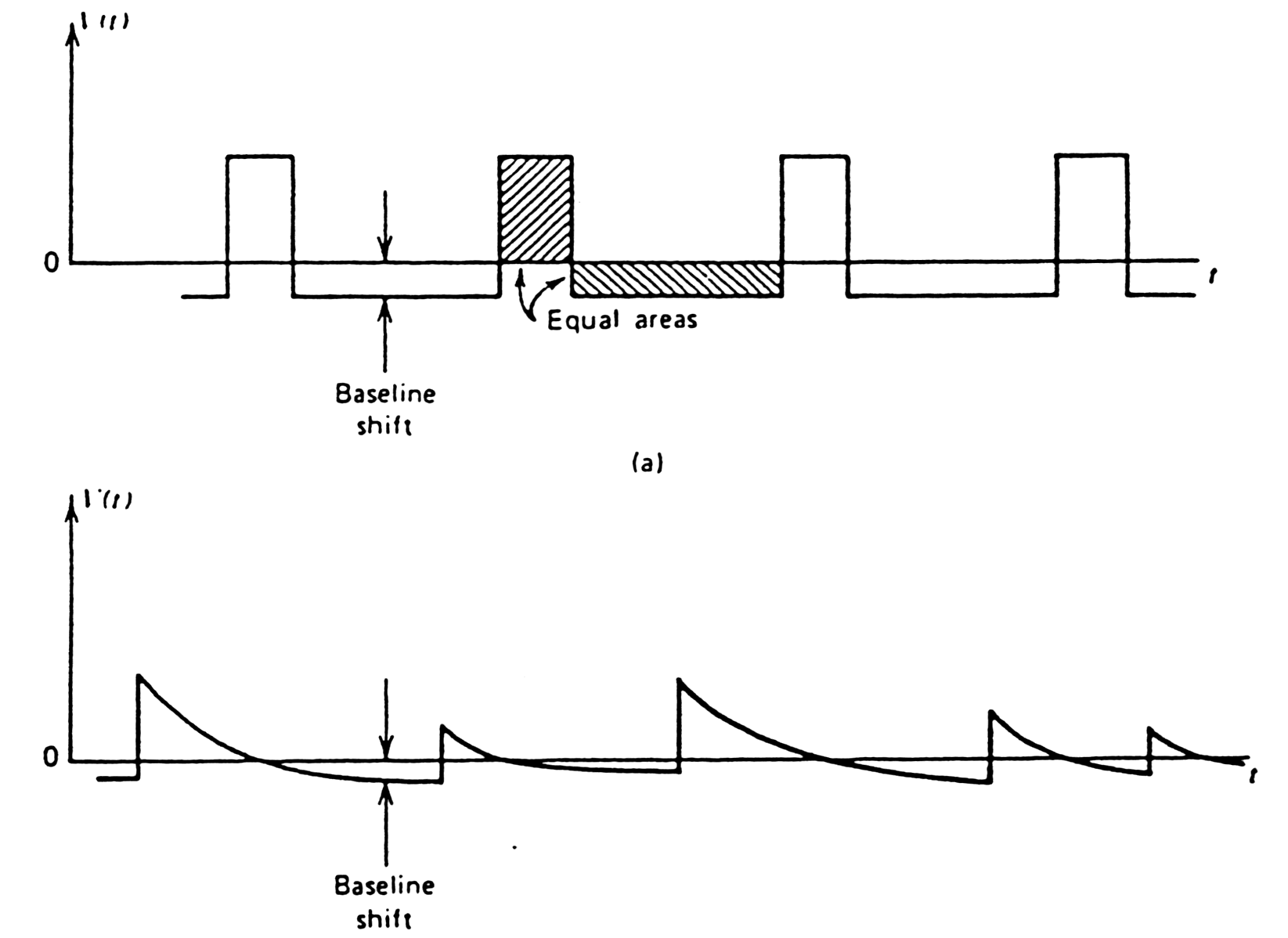 |
Fig. m-32
Baseline shift:
|
Baseline
restorer (BLR) reduces baseline shift.
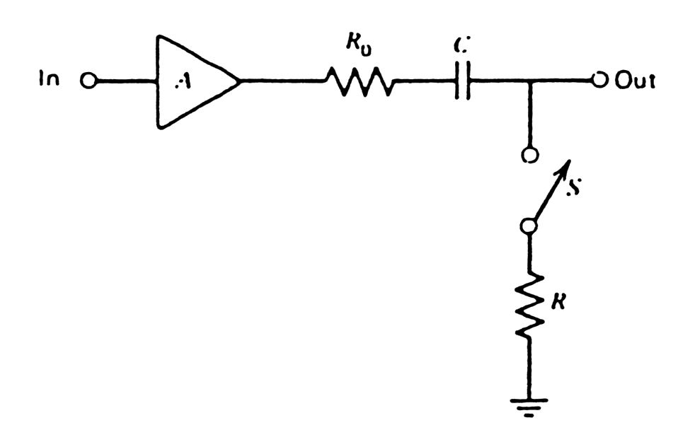 |
Fig. m-33
Basic principle of baseline restorer: Connect signal line to ground in absence of signal to establish baseline just to arrival of pulse. |
BLR are originally performed with diodes (passive restorer), today BLR circuits tend to include active loops with adjustable thresholds to sense presence of signal ("gated" restorer) + asymmetric charge and discharge time constants for the "memory" capacitor.
![]()
| Pile-up rejection |
Pile-up causes
false amplitude measurement.
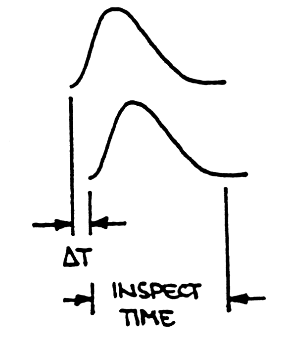 |
Fig. m-34
Two cases of pile -up false
amplitude measurement:
--> both amplitudes affected by superposition. In the case both pulses are rejected. Dead time: DT+inspect time (~pulse width); |
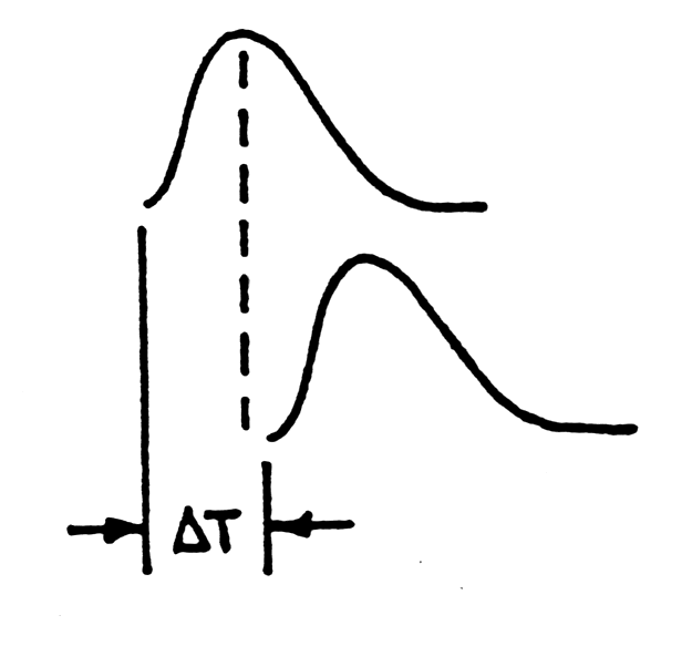 |
DT
< time to peak and DT < inspection time, i.e. time where amplitude of first pulse << resolution --> peak amplitude of first pulse is unaffected and second pulse is rejected only. No additional dead time is necessary if first pulse is accepted for conversion and dead time of ADC>( DT+inspect time) |
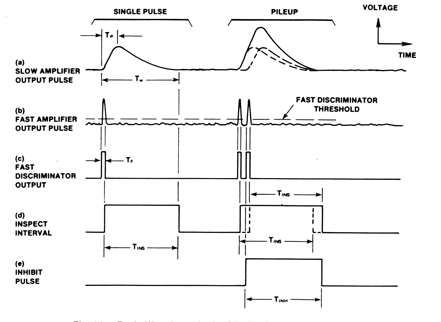 |
Fig. m-35 Basic
waveforms in the pile-up rejector.
|
When 2 gamma-rays (according to figure above) arrive at the detector within the width of the spectroscopy amplifier output pulse a pulse pile-up to form an output pulse of distorted amplitude can occur.
The pile-up rejector is implemented by adding a "fast" pulse-shaping amplifier with very short shaping time constant in parallel with the "slow" spectroscopy amplifier.
Fast discriminator is set above the much higher noise level => digital logic pulses.
The trailing edge of fast output triggers an inspection interval TINS pulse , that covers the width TW of the slow pulse.
If second fast
pulse arrives during TINS
an inhibit pulse is generated (prevents A/D analysis of the pile-up
event)
contribute to dead time of the spectrometry system:
|
TD =
|
TP+TW |
|
TW
-
|
width of the pulse above noise level, |
|
TP
-
|
time from start of the pulse until ADC detects the peak and closed its linear gate. |
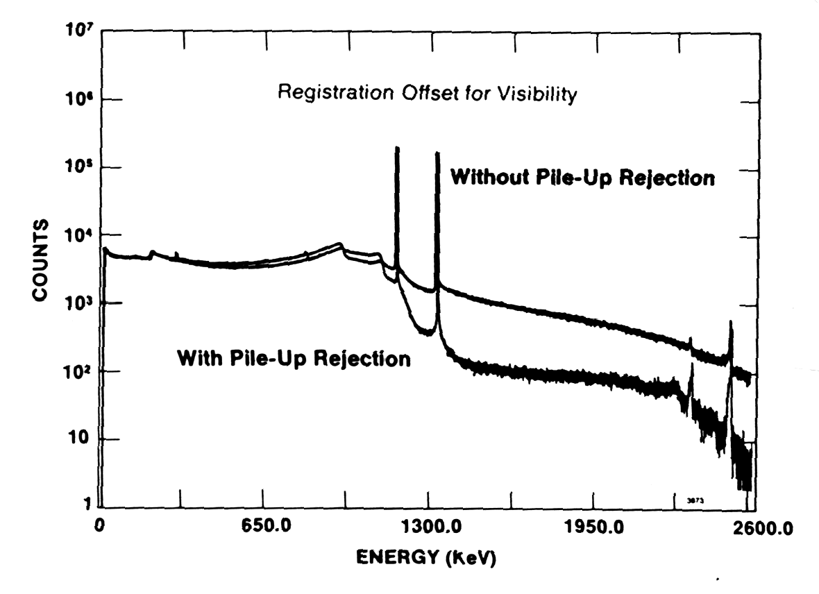 |
Fig. m-36 Demonstrations of Effectiveness of the Pile-Up Rejector in Suppressing the Pile-Up Spectrum with a Germanium Detector and a 60Co Spectrum at 50 000 count/s. |
![]()
| Noise |
In almost every area of measurement the ultimate limit of detectability of weak signals is set by noice - unwanted signals that obscure the desired signal. Even if the quantity being measured is not weak, the presence of noise degrades the accuracy of the measurement.
Noise- random variation in the output current of electronics circuits and amplifiers. These fluctuations in current are primarily due to the inherent particle nature of electrical current, and to variations in path, recombination rates, and diffusion caused by the randomness of charge movement. While the statistical average of diffusion current may be constant, on an instant-by-instant basis the diffusion rate may vary. At very low signal levels the signal current may be comparable in magnitude to the variation produced by such noise.
The noise has no specific frequency. Each impact of charges with atoms produces a very short energy pulse, which represents a very broad band of frequencies. Being random in nature, the distribution has a statistical effective power Pn .(Usefully interpreted signal has on time interval tj - ti its mean value, different from zero, but mean value of noise is zero!) Measurement of noise must be made over specified frequency band on power or voltage-square basis.
The noise power can be stated as Pn/D f - effective power per Hz at a center frequency, or Vrms/D f - effective voltage per Hz at a center frequency .
In a multistage amplifier, the noise power is attenuated by circuits or stages of amplifier. Because additive contribution of noise from the second stage to all noise is less than contribution of the first stage, it is conventional to refer noise rms voltage to the input an amplifier.
In this conclusions we suppose a proper grounding and shielding and the elimination of interface and pickup. Then the noise is applied to anything that obscures a desired signal, the term describing "random" noise of physical (often thermal) origin. Noise can be characterized by its:
- frequency spectrum;
- amplitude distribution;
- physical mechanism responsible for its generation.
Resistor
generates a noise voltage across its terminals.
The thermal noise is developed by the random thermal motion and impacts
of the charges and atoms in all conductors. Since is due to thermal
energies,
this noise is temperature dependent. It is also found to be uniformly
distributed
over all frequencies presently in use. (Noise whit a flat spectrum is
called "white
noise") The thermal noise due to a resistance R is:
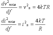
| Vn(rms)= VnR=(4kTRD f)0.5 |
The term SnR=4kTR
is called spectral
density of noise and is often used by describing properties of
this
type of noise too. (T - absolute temperature in degrees Kelvin, k -
Boltzmann's
constant, Df is
the
bandwidth in hertz). In graphical mapping of noise is often used
density
units like Vn/(Hz)0.5 (- Vn per root
Hz),
or Vn2/Hz (- volts squared per Hz).
 |
Spectral density of the termal noise |
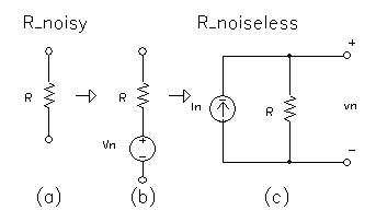 |
Fig. m-37a
Real "noisy" resistor R and
his equivalent circuit (spectral density 4kT) with "noiseless" R and
|
For example 10kW resistor has on open-circuits rms voltage of 1.3mV, measured with bandwidth Df=10kHz. A real resistor may be considered as equivalent thermal noise generator of rms voltage Vn (or source In ) in series (parallel) with noiseless resistor R.
The significance
of thermal noise is that
it sets a lower limit on the noise voltage in any detector or
amplifier,
having resistance. The noise
power is dependent on the frequency band Df
=>wide Df
gives more
noise => The bandwidth should be made as small as possible to get
reduced
termal noise.
An electric
current is the flow of discrete
electric
charges. The finiteness of the charge quantum result in statistical
fluctuation
of the current. The noise is uniformly distributed over frequency
spectrum.
(white noise as "the rain in a tin roof"). The noise energy increases
with
the current in device, so collector currents are maintained at a
few
hundred mA
for low noise application (IC min) :
| Inoise(rms)= In=(2e Idc D f)0.5 |
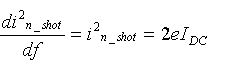 |
Spectral
density of the
shot noise
|
Shot
noise and Johnson noise are irreducible
forms of noise generating according to physical principles. Real
devices
have in addition to thermal and shot
noise
variation,
various sources of "excess
noise". This
noise
depends on many factors having to do with the construction of the
particular
resistor, including the resistive material (carbon-composition, metal
film,
wire-wound) and especially the end-cap connections. This noise has
approximately
a 1/f spectrum and is sometimes called "pink noise".
=> Base current noise in transistor is reduced to low level by
suitable
fabrication techniques. Flick noise seems largely confined bellow
1000Hz
and varies inversely with frequency.
Voltage and current noise
transistor
amplifier
It is
conventional to refer noise
voltages
to the input of an amplifier (although the measurements are
usually
made
at the output), i.e., to describe source noise and amplifier noise in
terms
of microvolts at the input that would generate the observed output
noise.
This makes sense when you want to think of the relative noise added by
the amplifier to a given signal, indipendent of amplifier gain;
it's
also realistic, because most of the amplifier noise is usually
contributed
by the input stage.
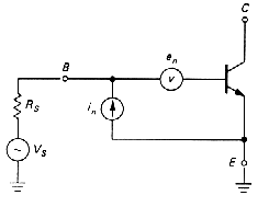 |
Fig. m-37b The noise
model of an amplifier:
|
The noise generated by an amplifier is easily described by a simple noise model (fig. above in which :
- en - represents noise voltage source in series with the input, and
- in - input noise current ((in bipolar trasistor).
| ea (rms) = [ en2 + (RS in)2 ]0.5 |
The two terms are the amplifier input noise voltage and the noise voltage generated by the amplifier's input noise current passing through the source resistance RS .Since the two terms are usually uncorrelated , their squared amplitudes add to produce the effective noise voltage seen by the amplifier. For low value of resistance RS noise voltage en dominates, whereas for high RS the noise current generally dominates. The fact that en drops and in rises with increasing collector current provides a simply way to optimize transistor operating current to give lowest noise whit given source.
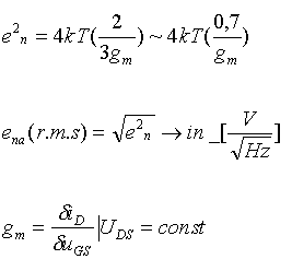
JFET noise
voltage en is
essentially thermal noise of channel resistance given approximately by
| en2 = 4kT(0.7/gm) | |
| where - 1/gm | - inverse transconductance takes the place of resistance. (gm- characterizes the change in current per volt change in gate input => slope of the transfer curve). |
| For the JFET, where is the current noise component in very low depends en2 first of all on the inverse transconductance of the transistor gm: |
 |
![]()
According the figure bellow noise current and voltage sources can be described by their spectral densities, which depends on:
- Detector bias shot current Ib (part (a) on fig. below) ;
- Shunt resistance thermal noise (load resistor R of the detector - part (b) on fig. below);
- Series resistance thermal noise ( for JFET RS=0,7/gm - part (c) on fig. below);
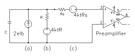 Fig. m-38 The detector current signal source is on fig. represented with capacitor C only. The noiseless detector signal source has added to it an irreducible noise voltage from the Johnson noise of its source resistance and from noise current shot noise. |
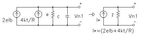 |
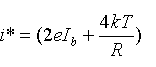
| Equivalent input noise circuit in fig. up depends on current: |
 |
| Then noise on the output of the equivalent voltage circuits, based on the input impedance Z (R parallel with C) is: |
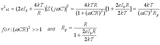 |
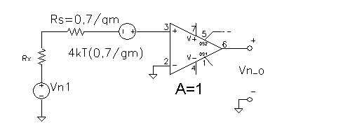 Fig. m-39 Fig. m-39 |
 |
Then the
equivalent noise charge:
 |
consist of parts:
- The "parallel" noise component, proportional to shaping time constant ti =td =t and independent of capacitance of the detector C.
- The "series" noise component, proportional to capacitance of the detector C and calculated proportional ~1/t .
- Maximal resistance Rp and minimal bias current Ib (-> for extremely small bias currrent is recomending to work at low temperatures).
- Minimal resistance RS,- can be accomplished by FET with high gm, or by connecting 2, 3 FET in parallel (individual selection FET according to minimal flicker noise component 1/f too).
 |
True in general must be experimentally checked, e.g. for system with Si - barrier detector can be optimal t~0,5 - 1ms , and for germanium or Si(Li) detector t~6 - 20ms.
Next figure
illustrates dependence parallel and series
component to total noise of the preamplifier. Short time constant t
is dominant for series component of the noise and long time constant
again
for parallel component (which depends on thermal Rp~R, thus
on detector leakage Ib or gate leakage current of FET).
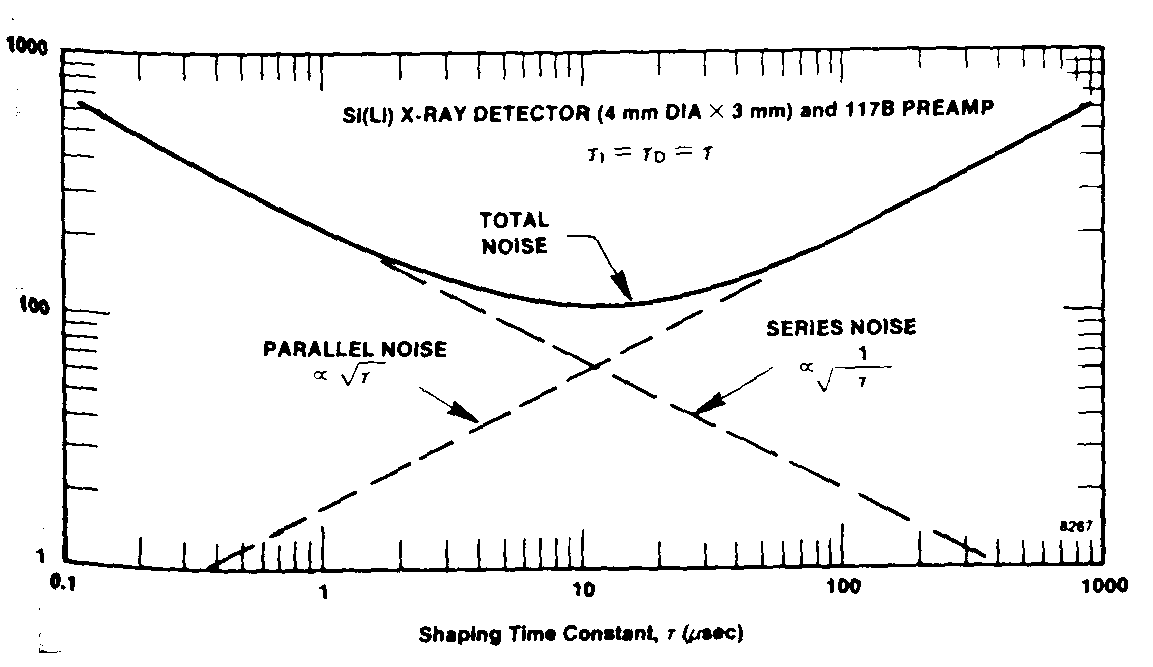 |
| Fig. m-40 The dependence of preamplifier noise contribution on the amplifier shaping time constant. |
For comparing purpose the system noise can be expressed:
- as "noise" charge Qn in Coulombs ;
- in noise electrons Nn= Qn /e, where e is electron charge 1,6. 10-19C;
- or in energy units (eV, keV), e.g. FWHM (usually requires specification of detector material too).
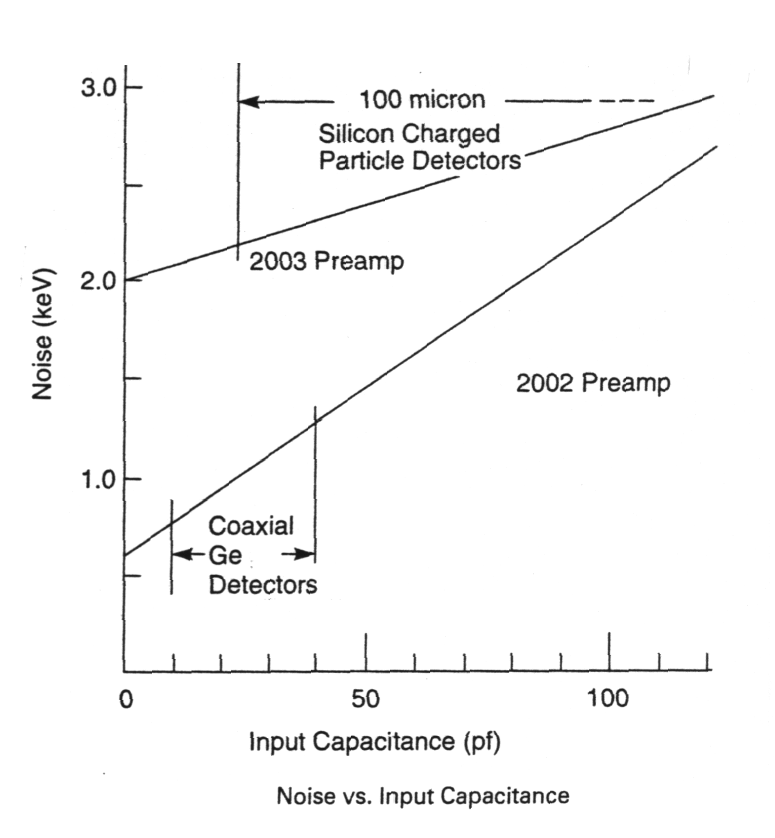 |
Fig. m-41
Noise (expressed in FWHM keV) vs. input capacitance C of detector dependence for 2 type of preamplifiers. |
![]()
| Preamplifier |
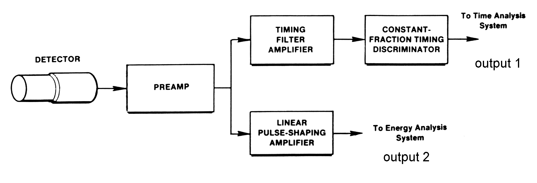 |
| Fig. m-42 Application of preamplifier in the timing (output 1) and energy (output 2) measurement. |
Preamplifier is
located close to the detector
and accepting signal from detector preserves max S/N ratio whit
minimum
shaping, or sometimes a fast rise time output pulse for good time
resolution
measuremnt too.
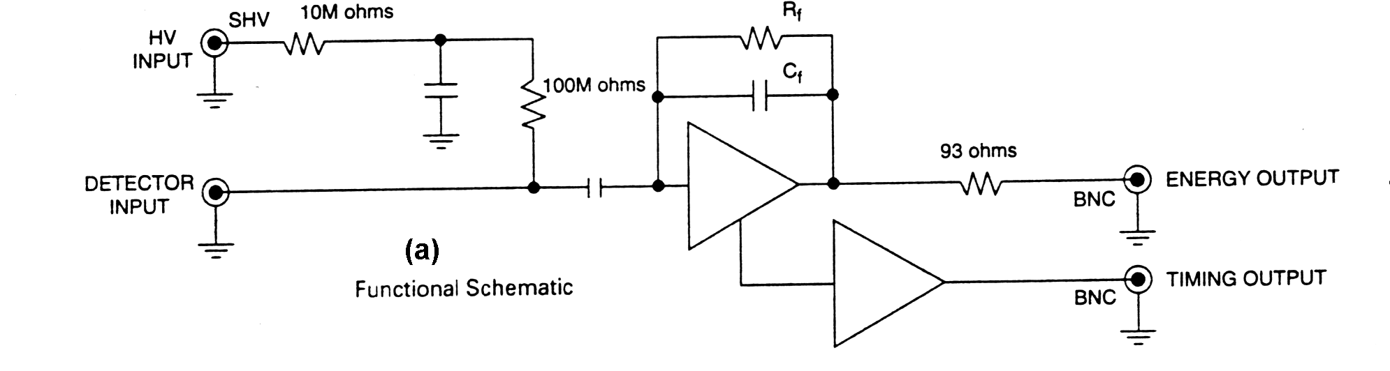 |
Fig. m-43
Functional schematic of preamplifier with fast/slow output. |
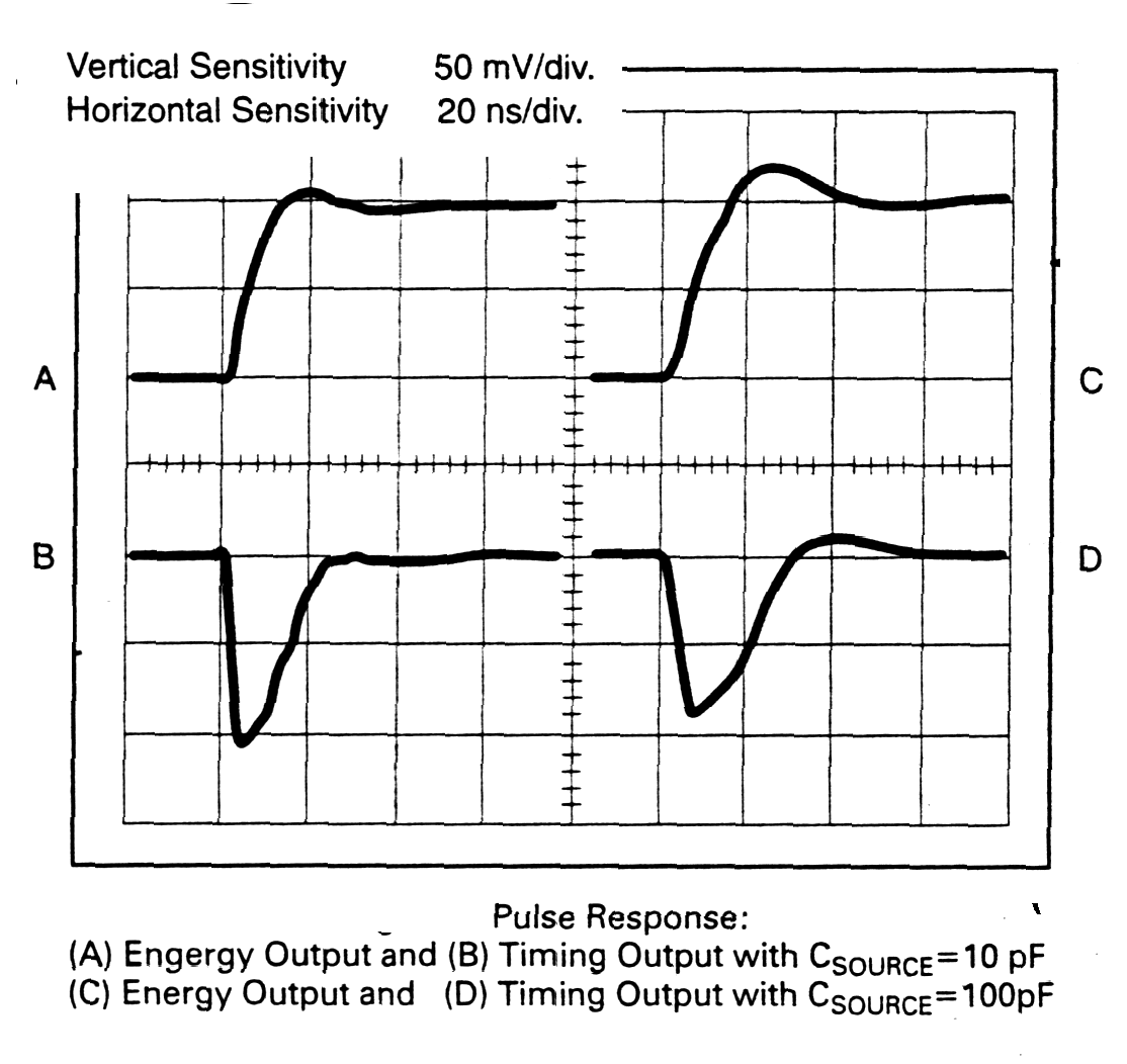 |
Fig. m-44
Pulse response on energy / timing output. |
The optimum configuration of preamplifier in system depends on characteristics of the detector and type of signal processing following after.
There are generally used 3 type of preamplifiers:
- Voltage preamplifiers;
- Current preamplifiers;
- Charge sensitive preamplifiers.
1. Voltage - sensitive
preamplifier:
It has high impedance input. It accept the signal from circuit of parallel combination of detector capacitance and its input resistance and responds with a low-impedance output signal, suitable for driving a long cable to the linear amplifier. It is not widely used for energy spectroscopy applications because its gain dependent on detector capacitance (CD does not remain constant during bias voltage change) => makes broader the peak width.2. Current - sensitive preamplifier:
It has low impedance input (R~100W) to convert fast current pulses (f.e. from the anode of a PM to a voltage pulse). It is used when fast timing is desired. The output accepts several meter coax without shape distortion. e.g. the input resistance 100W preamplifier with the gain 10 has sensitivity Uout/Iin=500 mV/mA (Uout - voltage amplitude of the output pulse, Iin-- current amplitude of the input pulse.)3. Charge - sensitive preamplifier:
It is preferred for most energy spectrometric applications. Preamplifier is mounting close to detector, thus reducing input capacitance caused by cabling, decreasing microphone noise, ground loop and radio-frequency pickup. The signal from a semiconductor detector or ion chamber is a quantity of charge, delivered as a current pulse, lasting from 1ns to 10us, depending on type of detector and its size. For most applications the quantity of charge and/or the time of occurrence of an event are the parameter of interest.
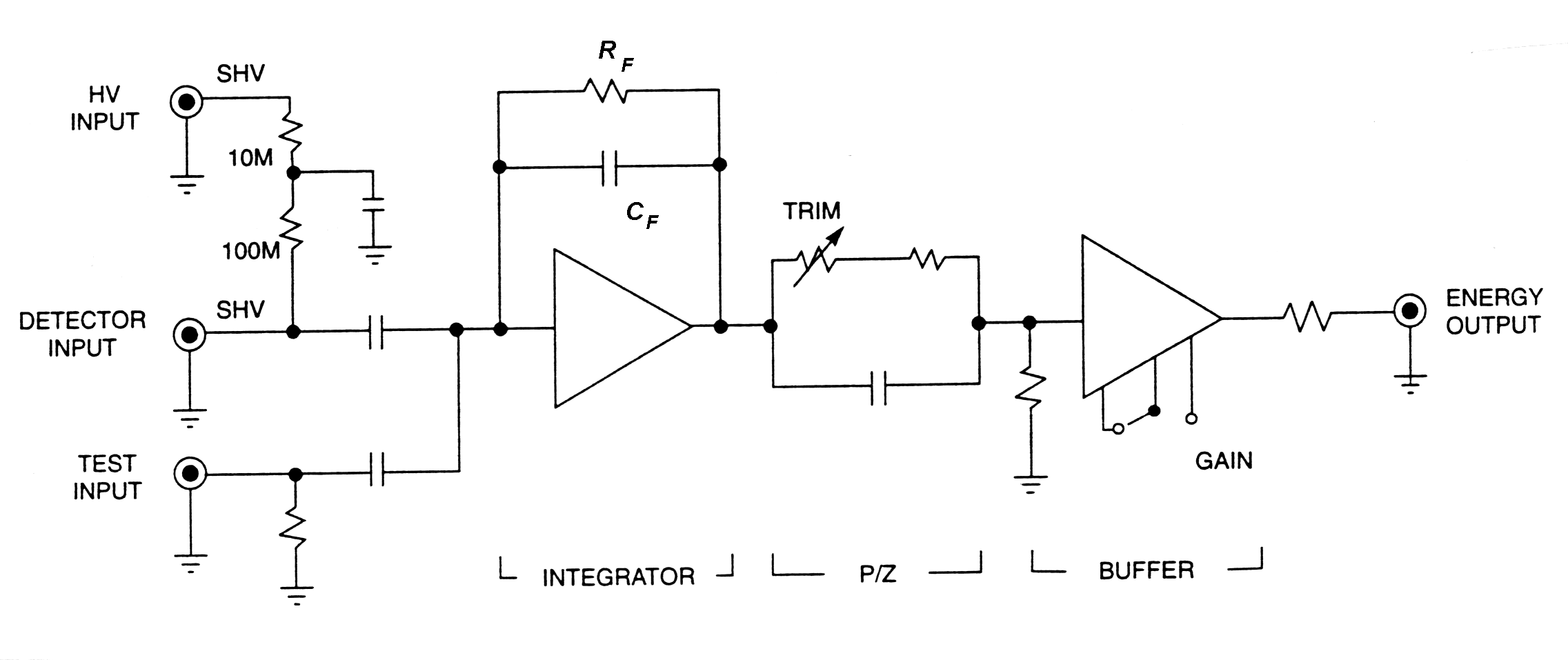 |
Fig. m-45 Typical
charge - sensitive preamplifier
consists of 3 parts:
|
Charge sensitive preamplifier integrates the charge QD on its feedback capacitor Cf . Its gain Aq~Vo/QD~1/CF is not sensitive to variations of detector capacitance. The rise time of its output pulse is equal to the detector current pulse width in ideal case.
Voltage from
preamplifier output Vo~QD/CF.
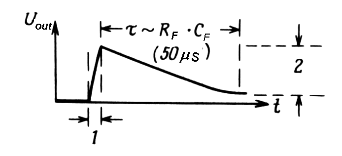
The decay time constant tF=RFCF
(CF~0.1 to 5pF). Feedback resistor RF is a noise
source and is made as large as possible with the signal energy rate
product
and the detector leakage current in the direct-coupled system.
 |
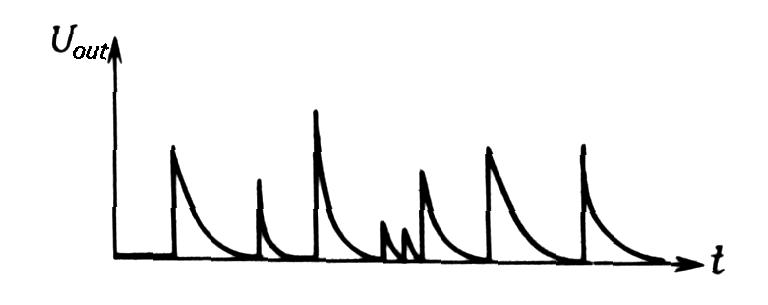 |
Fig. m-46
Typical shape of output pulse
from charge - sensitive preamplifier:
|
Fig. m-47
The same pulse output in other time scale (at middle counting rate). |
Sensitivity (usually is expressed in mV/MeV ) Vo/E =e/(eCF) to energy E deposited in given detector material. The charge released by the detector is a function of the gamma - ray or particle energy and the detector material QD=eE/e (e - the amount of energy required to produce e.g. an electron-hole par in the detector.)
Preamplifier noise depends on FET, resistance to the input, input leakage current from detector and FET and total capacitance at the input (CF, CD).
The noise can be
measured in the system shown on
next figure.
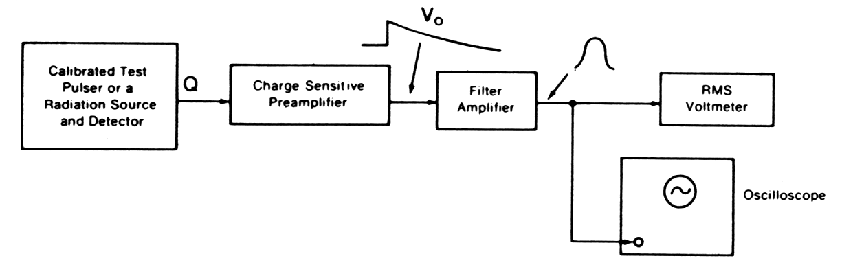 |
| Fig. m-48 System for Measurement Charge Sensitive Preamplifier Noise |
- At first system gain Vp/E must be determined. Charge Q, equivalent to the known energy E, is injected into preamplifier by detector radiation source or step pulse generator connected through a capacitor (Vp - pulse amplitude from the charge Q).
- Then noise can be determined by measuring out the voltage Vrms at the output of the filter amplifier:
| FWHMnoise.=2.35 VrmsErms/ Vp [ in keV] . |
![]()
| Linear pulse-shaping amplifier |
Linear pulse-shaping amplifier is special type of wide-band amplifier, which is used with scintillation, silicon charge particle detectors for energy spectroscopy measurement.
- Primary purpose to magnify the amplitude of the preamplifier output pulse from the mV range into the 0.1 - 10V range (ADC level).
- Shapes the pulses to optimize the energy resolution.
- Minimize the risk of overlap between successive pulses.
- Baseline ensure that the baseline between pulses is held rigidly at ground potential in spite of changes in counting rates or temperature
For detector with very short charge collection times, the rise time of the preamplifier output pulse is controlled by the amplifier itself, and the rise time is usually in the range from 10ns to 100ns.
For detector with
long charge collection times, such
as NaI(Tl) detectors, proportional counters, coax Ge - detectors, the
output
rise time of the preamplifier is controlled by the detector charge
collection
time. The output rise time can range up to 700ns, for large Ge -
detectors,
and ~500ns for NaI(Tl) detectors.
Conflict with the need of handling high counting rates and optimum energy resolution
The fast amplifiers – tries for minimal degradation of rise time => good time resolution.
The slow or wide-band linear amplifiers, used with scintillation, silicon charge particle detectors for energy spectroscopy purpose apart from magnify the amplitude of the preamplifier pulses are assign to :
- Shape the pulses for optimizing S/N ratio to optimize the energy resolution:
- CR - RC pulse shaping.
- Semi-Gaussian pulse shaping.
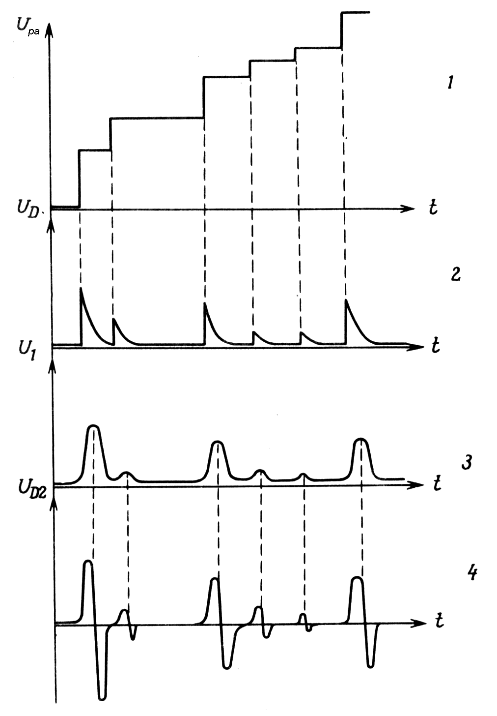 |
Fig. m-49
Typical CR - RC pulse shaping in linear amplifier:
|
- Minimize the risk of overlap between successive pulses by:
- Pole-zero cancellation (has a sense in the first stages of amplification, e.g. in preamplifier).
- Unipolar versus bipolar shaping (by height counting rates is bipolar shaping performed)
- Base-line restoration (is performed in the last stages of amplification).
- Pile-up rejection.
 |
| Fig. m-50
Illustration of baseline shift vs. counting rates. Simple diodes BLR or active fixation BLR can be used to minimize fluctuations in baseline shift due to random rate. |
![]()
| Back to menu |