 |
Pulse processing and Analyses
Dušan Kollár, |
|
|
|
|
|
Amplitude (Pulse Height) Measurements |
|
|
Frequency and time response of amplifiers |
|
|
Detector equivalent circuits |
|
|
Nuclear detector analog signal processing |
|
|
ADC - digitization of pulse high |
|
|
Timing measurement |
|
|
Time interval measurement |
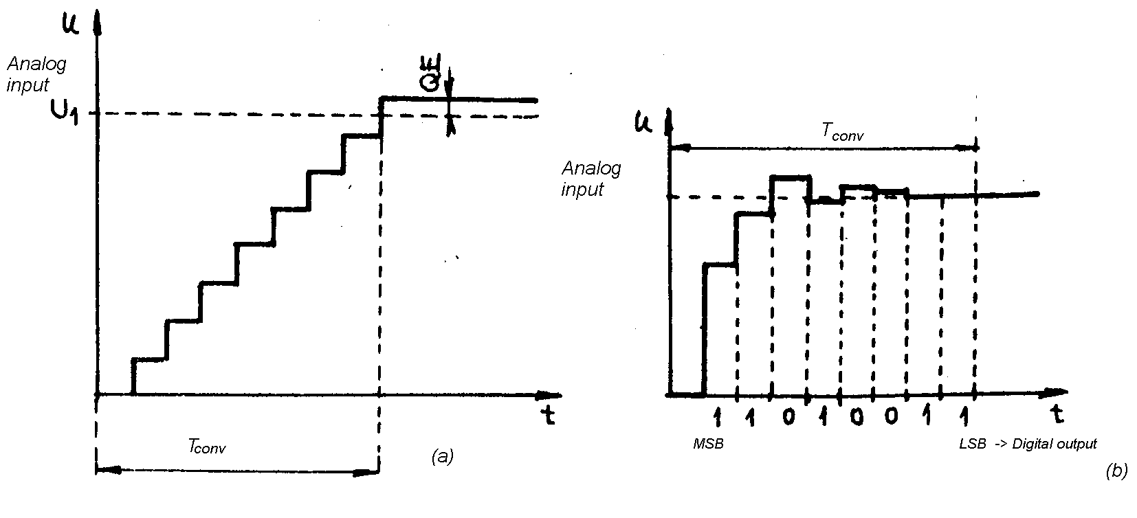
| Digitization of pulse high |
Ideal ADC:
| Fig. m-51 | 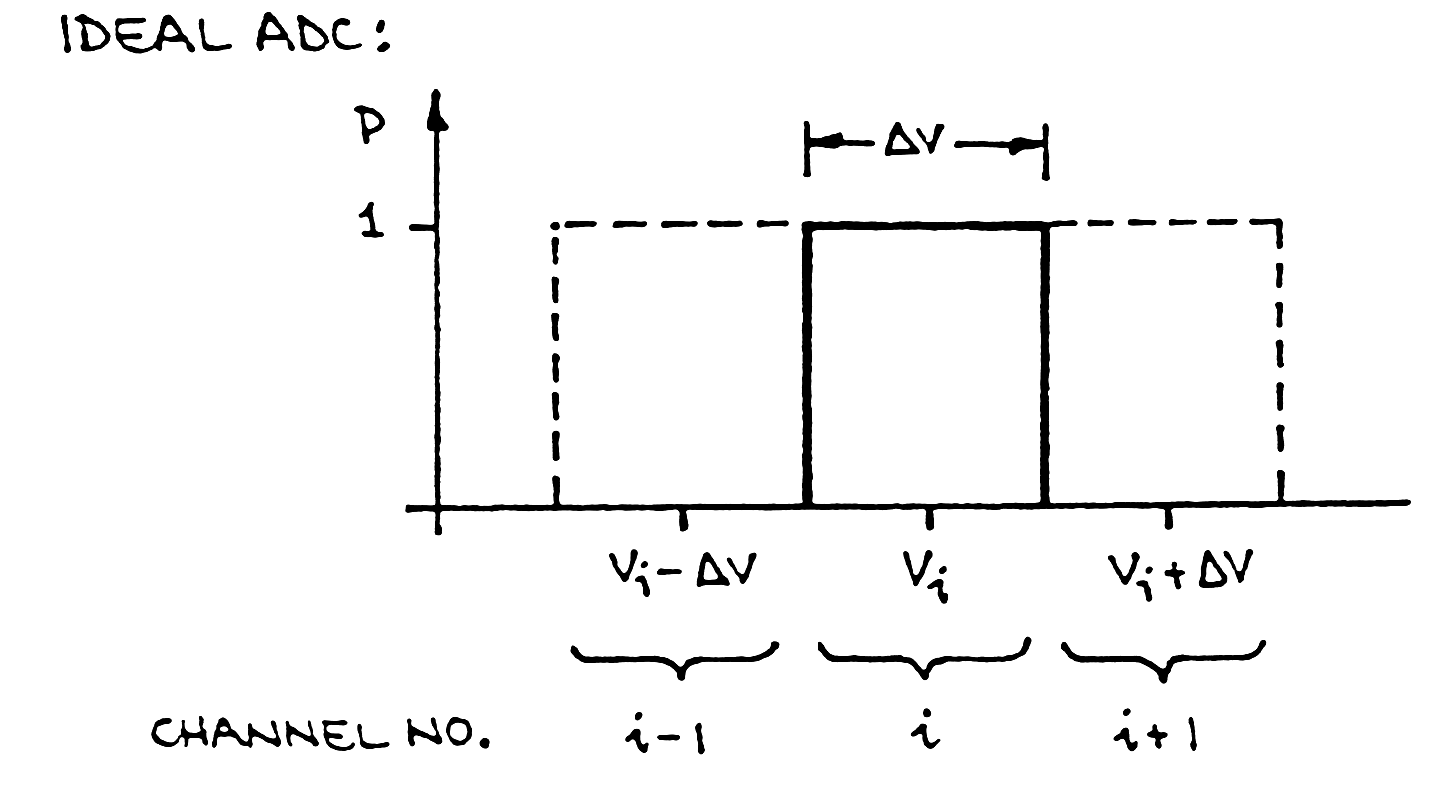 |
Measurement accurancy:
- If all counts of a peak fall in one channel, then the resolution is DV.
- If the counts are distributed over sevrel ( >4 or 5) channels, peak fitting can yield a resolution of 10-1….10-2DV.
-
- Resolution;
- Differential non-linearity ;
- Integral non-linearity;
- Other common errors (offset, scale error, non-monotonicity;
- Conversion time;
Stability;
| Resolution |
Simplistic assumption: resolution defined by number of output bits; e.g. 13 bits => DV/V=1/8192=1,2.10-4.
True measure: channel profile
Plot probability vs. pulse amplitude that a pulse height corresponding to a specific channel is actually converted to that address.
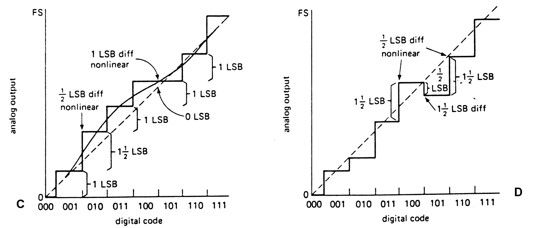
| Differential non linerity - DNL |
DNL is measure of equality of channel widths over the range of the ADC. DNL is computed as max. deviation DViof the counts in any of the channels from the average counts<DV>in all channels, expressed as the percentage of the average counts
Typically DNL for a 100MHz
Wilkinson ADC: <+- 1% max.
Note: A good instrumentation ADC
specified with an accuracy of +- 1LSB may have DNL = 20% to 50%.
| Integral nonlinerity -INL |
INL - deviation of recorded amplitude from input amplitude.
Typically values for modern ADC's: 0,01 to 0,1% (~ 1 -10 channels for 8k). Today SW correction commonly used.
| Other common errors |
Next figures illustring the definitions of
common digital conversions errors (offset, scale error, non-monotonicity
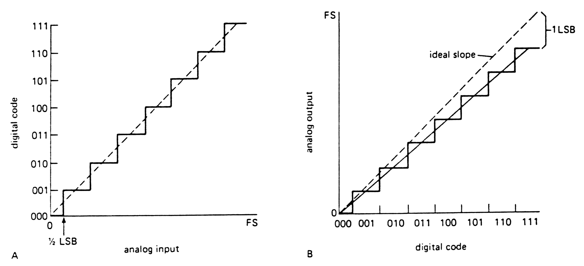 |
Fig. m-52
|
 |
| Count rate performance |
Problem of
spectroscopic resolution generaly due to baseline
shifts with event rate (however, crosswalk from digital to analog
circuitry within ADC can also cause problems). Effect is important when
rate changes during measurement (radioactive decay, beam fluctuations at
accelerators) . So the random rate fluctuation instantaneously leads to
spectral broadening.
| Examples (measurements performed with random rates): |
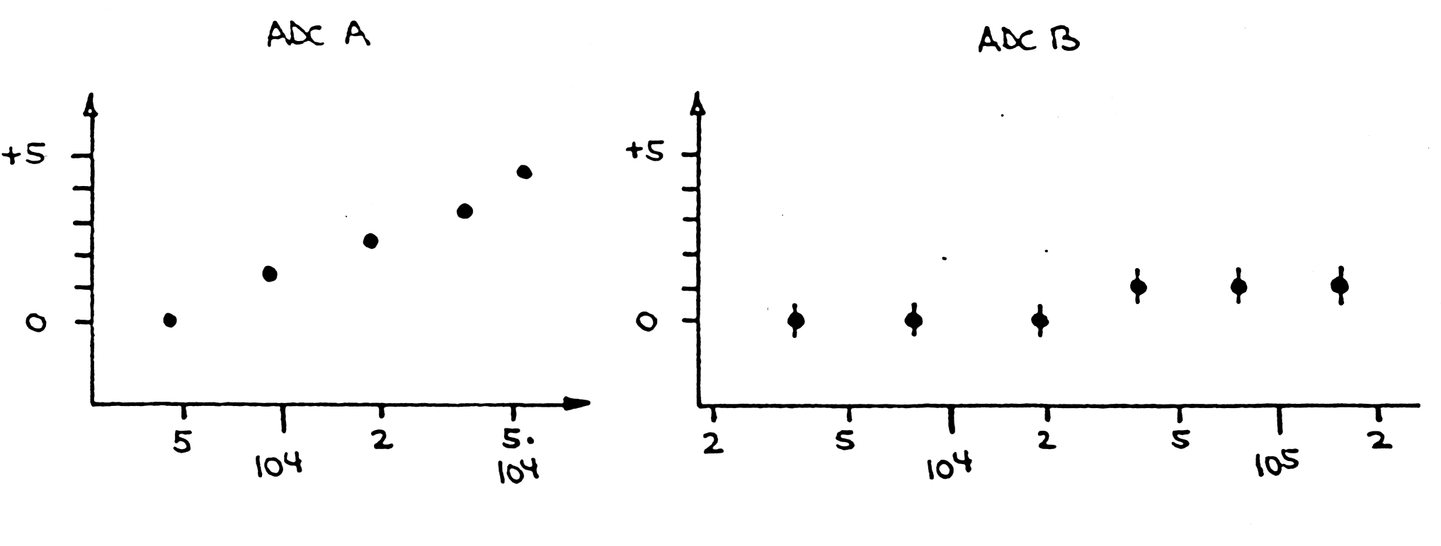 |
| Fig. m-62 ADC A) inadequate for high resolution gama ray spectroscopy |
Dead time of the A/D conversion is the sum of next three times:
- signal acquisition time ( --> time to peak + const)
- conversion time ( --> can depend on pulse hight)
- read-out time to memory ( --> usually negligible in MCA`s, but dominant as a rule in multiparameter computer based systems).
| Conversion time |
When detector, preamplifier, spectroscopy
amplifier and ADC are combined to form a spectroscopy system the dead
times of the amplifier and the ADC are in series => extending dead
time. When ( as in illustration fig.).
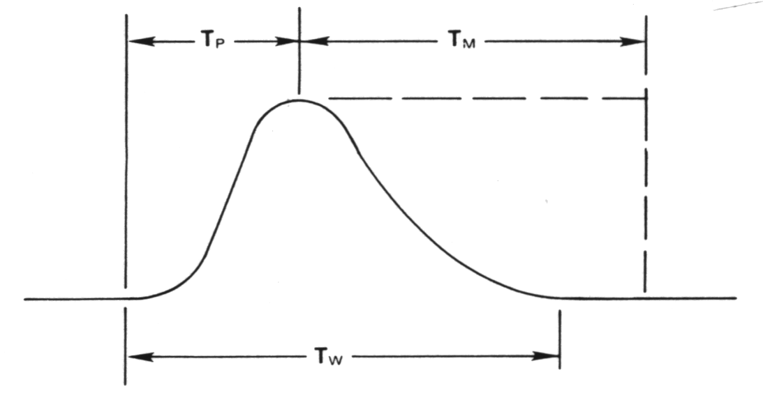 |
Fig. m-63 The sources of dead time with an amplifier and ADC. |
|
|
TW -
|
width of the amplifier pulsemeasuredat the noise discriminators threshold. |
|
TP -
|
time from
start to point which the ADC detects peak amplitude and close the linear gate. |
For successive approximation ADC TM is the fixed conversion time of the ADC and includes the time required to transfer the data to the subsequent memory.
For Wilkinson ADC the
value of Dead time (non extending):
TM = (Nc/fc) +
TMC,
where
|
fc -
|
clock frequency |
|
TMC -
|
memory cycle time |
For f=50 - 400 MHz, TMC~0,5us -
2us for 8k ADC, TM~20us - 165us => long time!!
DNL<1%T
At high counting rates, it is desirable to
have an ADC conversion time that is less then the time taken for the
amplifier pulse to return to the baseline after peak amplitude.
| Stability |
Stability vs. temperature + time usually adequate with modern electronics in laboratory environment (incl. Beam areas at accelerators). Note that temperature changes within module are typically much smaller than ambient.
However: highly precise + long term measurements require spectrum stabilization to compensate for changes in gain + baseline of overall system.
Technique: using precision pulsers
place a reference peak at low at high end of spectrum:
| (peak position 2) - (peak position 1) | --> gain, then |
| (peak position 1) or (peak position 2) | --> offset |
Traditional implementation: hardware,
spectrum stabilizer module today easier to use software to determine
corrections. These can be applied to software calibration or hardware
(simplest and best in ADC circuitry).
| DAC - techniques |
DAC - convert a quantity
specified a s binary (or BCD) number to voltage or current proportional
to the value of the digital input. There are a number of popular methods:
| Scaled resistors into summing junction |
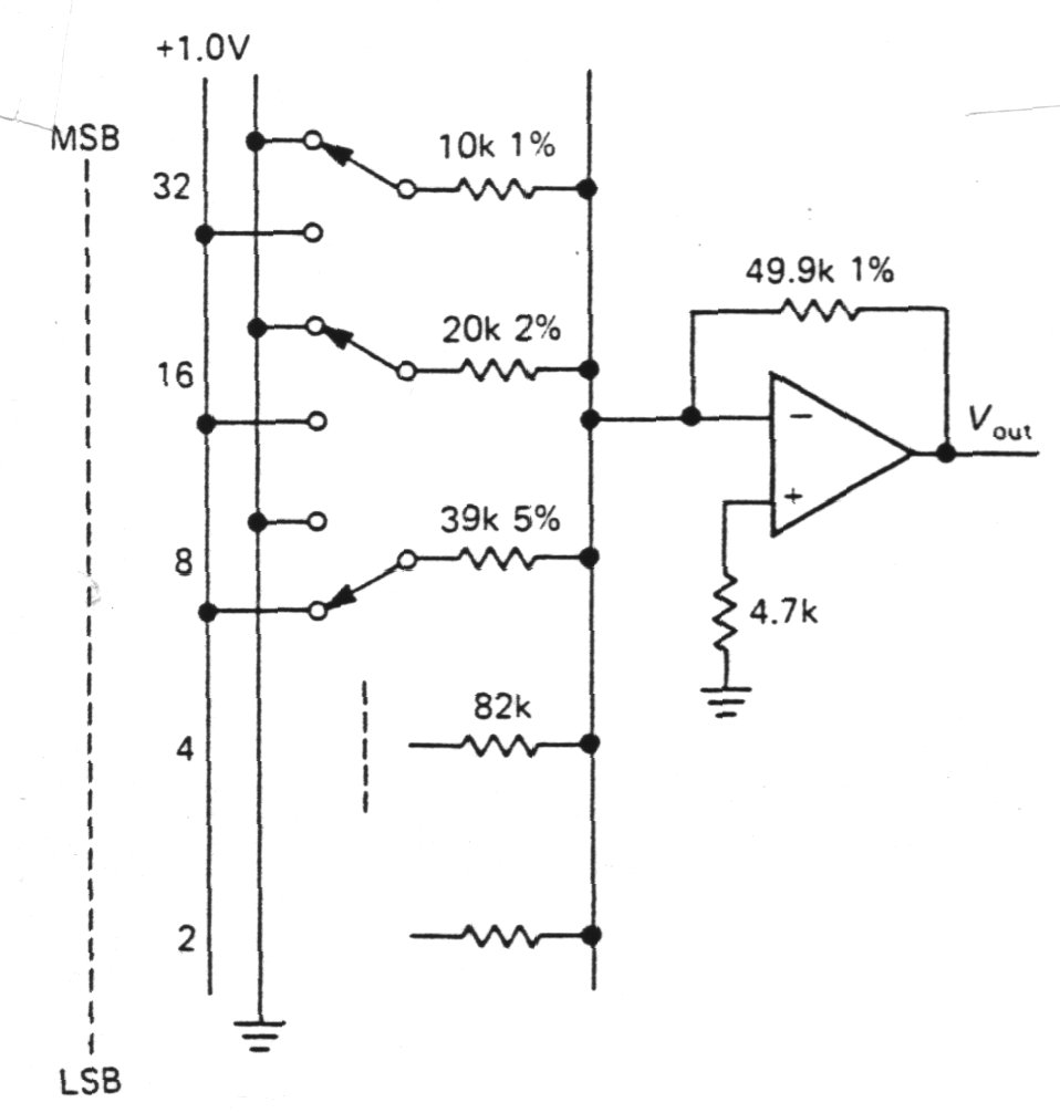 |
Fig. m-53 Scaled resistor DAC. Drawback: Height accuracy chosen bin weighted R!!! |
By connecting a set of resistors
to an op-amp's summing junction get an
output proportional to a weight sum of the input voltages.
| R - 2R ladder |
Set of resistors of two values only. Switch circuits in realized with transistors
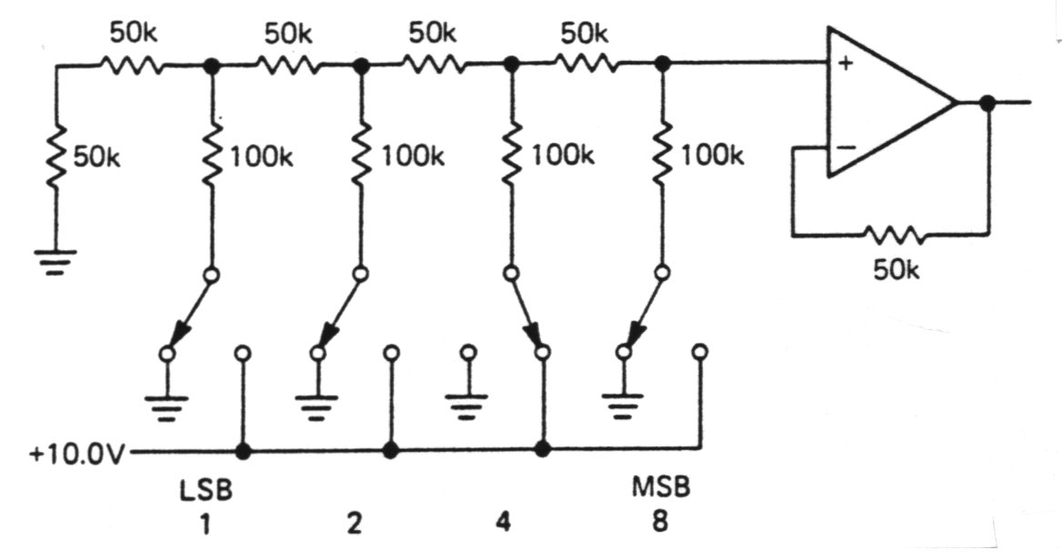 |
Fig. m-54 R-2R ladder DAC. |
| ADC - techniques |
- Flash ADC ( parallel encoded)
- Successive approximation
- Slope integration (Single / Dual)
| Flash ADC |
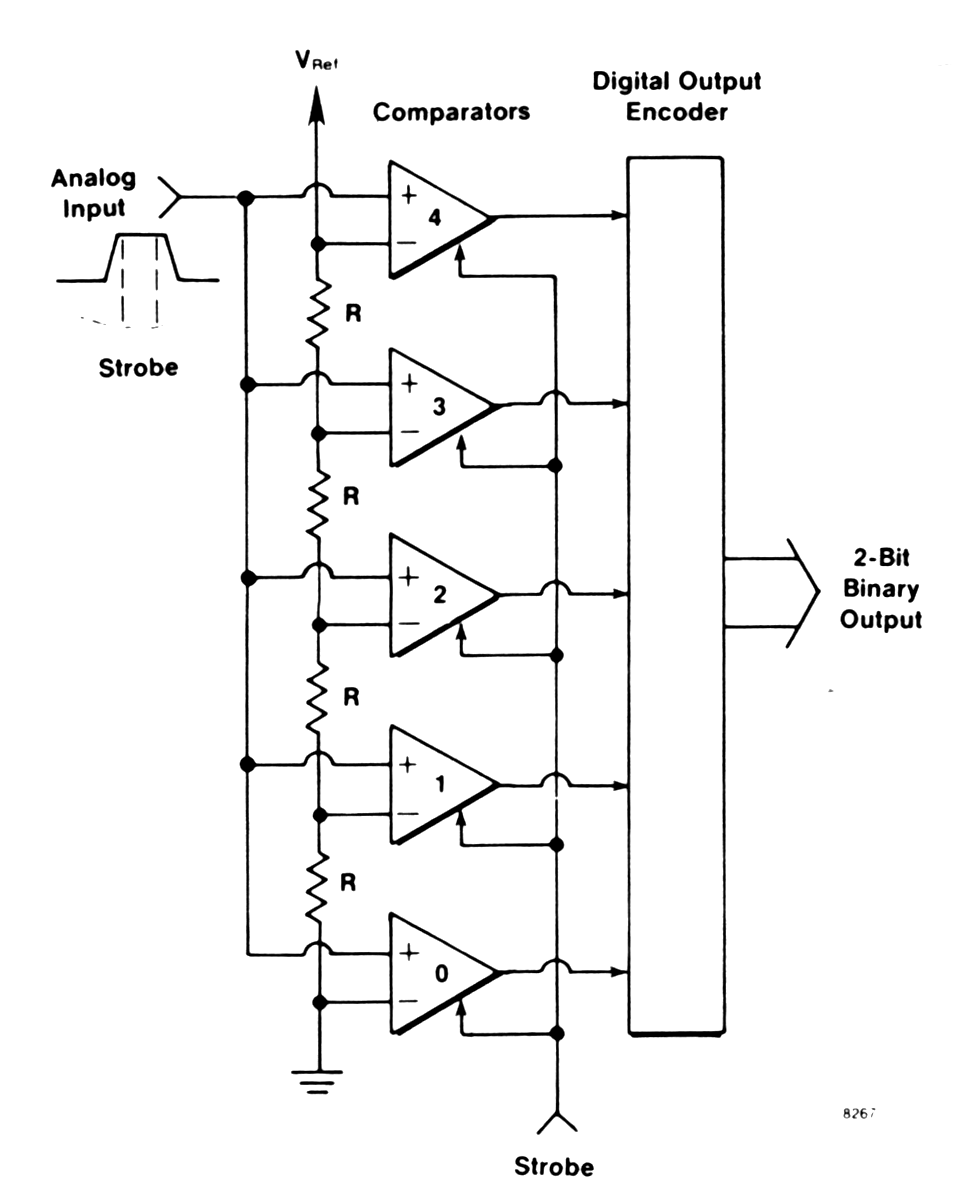 |
Fig. m-55 The principle of flash ADC. Advantage: short conversion time Drawback: Limited accuracy (currently 10bit) Power consumption Differential non linearity |
Parallel encoder - fastest method of
A/D conversion. The input signal voltage is fed simultaneously to
one input of each n comparators (8 bit requires 256
comparators), the other inputs of which are connected to n - equally
spaced reference voltages. A priority encoder generates a digital
output corresponding to the highest comparator activated by input
voltage. The delay time from input - output equals the sum of
comparator plus encoder delays ( < 20 ns, 10 ns available). Value of
resistors in divider chain ( in IC's) not critical (only matching ).
| Single slope ADC |
 |
| Fig. m-56 The principle of ADC (At the the beginning of the conversion is the track and hold capacitor C held at ground.):
|
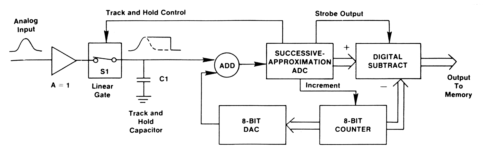
| Successive approximation ADC |
In successive approximation ADC (according
to fig.) during the rise of the analog input pulse the switch S1 of
linear gate is closed and voltage Uc1 tracks the rise of the
input signal.
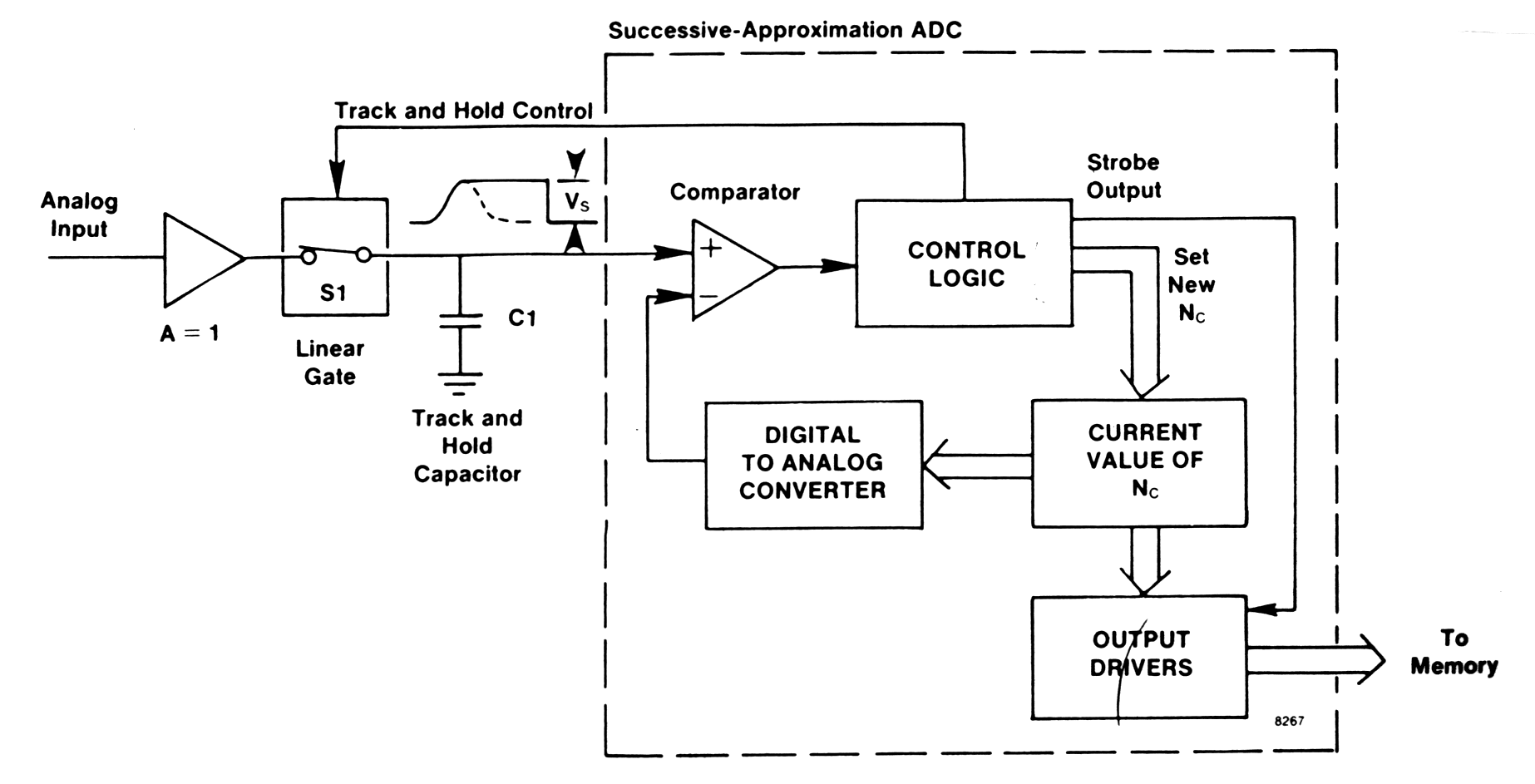 |
| Fig. m-57 The basic circuits used with a successive - approximation ADC. |
When input signal reach maximum amplitude, linear gate switch S1 is opened, leaving C1 holding the maximum voltage of the input signal. After detection of the peak amplitude of the input pulse, the successive-approximation ADC begins its measurement process.
In this technique you try various output codes in following turn:
- At the beginning computer sets all bits initially to 0
- Then each bit in turn, beginning with MSB, is set provisionally to 1 and the output codes are feeding into DAC and comparing the result with the analog input via comparator. If D/A output does not exceed the input signal voltage, the bit is left as 1, otherwise it is set back to 0. For an n - bit A/DC, n such steps are required.
Advantage: speed => fast ( 1ms to 50ms width accuracy 8 - 12 bits IC's ( monolithic + hybrid) available.
Drawback: DNL (Typically 10 - 20%)
(The resistors that set DAC output must be extremely accurately pick and choose. For
DNL < 1% for 12 bit (8k) ADC accuracy < 2,4. 106
| Wilkinson ADC - Dual slope ADC |
Dual slope conversion cycle consist of:
- capacitor charge time (fixed ) with a current I~Uin;
- capacitor discharge time (by a constatnt current, in time Dt2~Uin depending on pulse hight Uin)
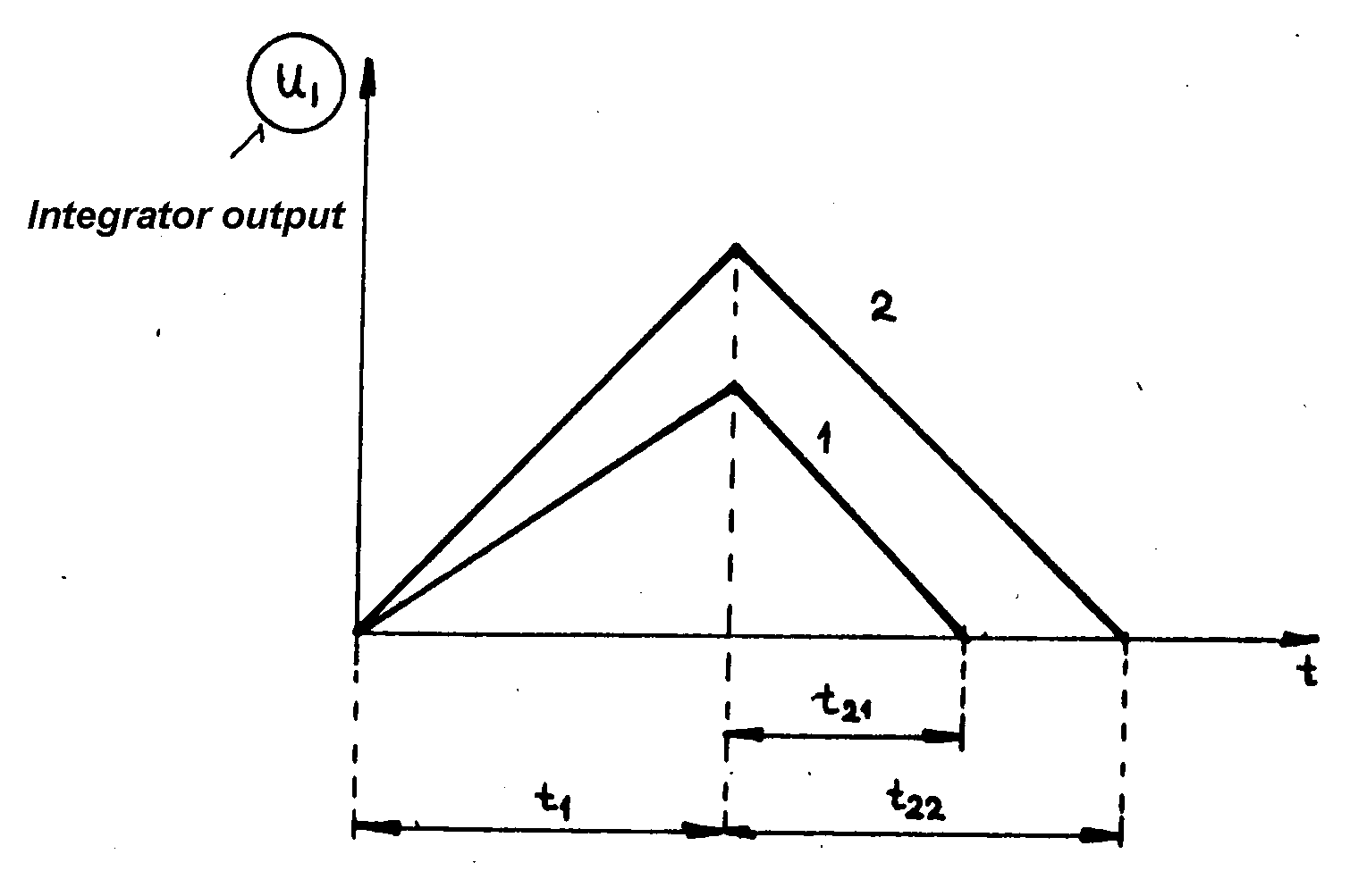 |
Fig. m-58 Dual slope conversion cycle: t1 - capacitor C is fixed time charged with current I~Uin. t2 - capacitor C is discharged by constant current during time t2~Uin. |
Signals in Wilkinson ADC
ilustrate next figure.
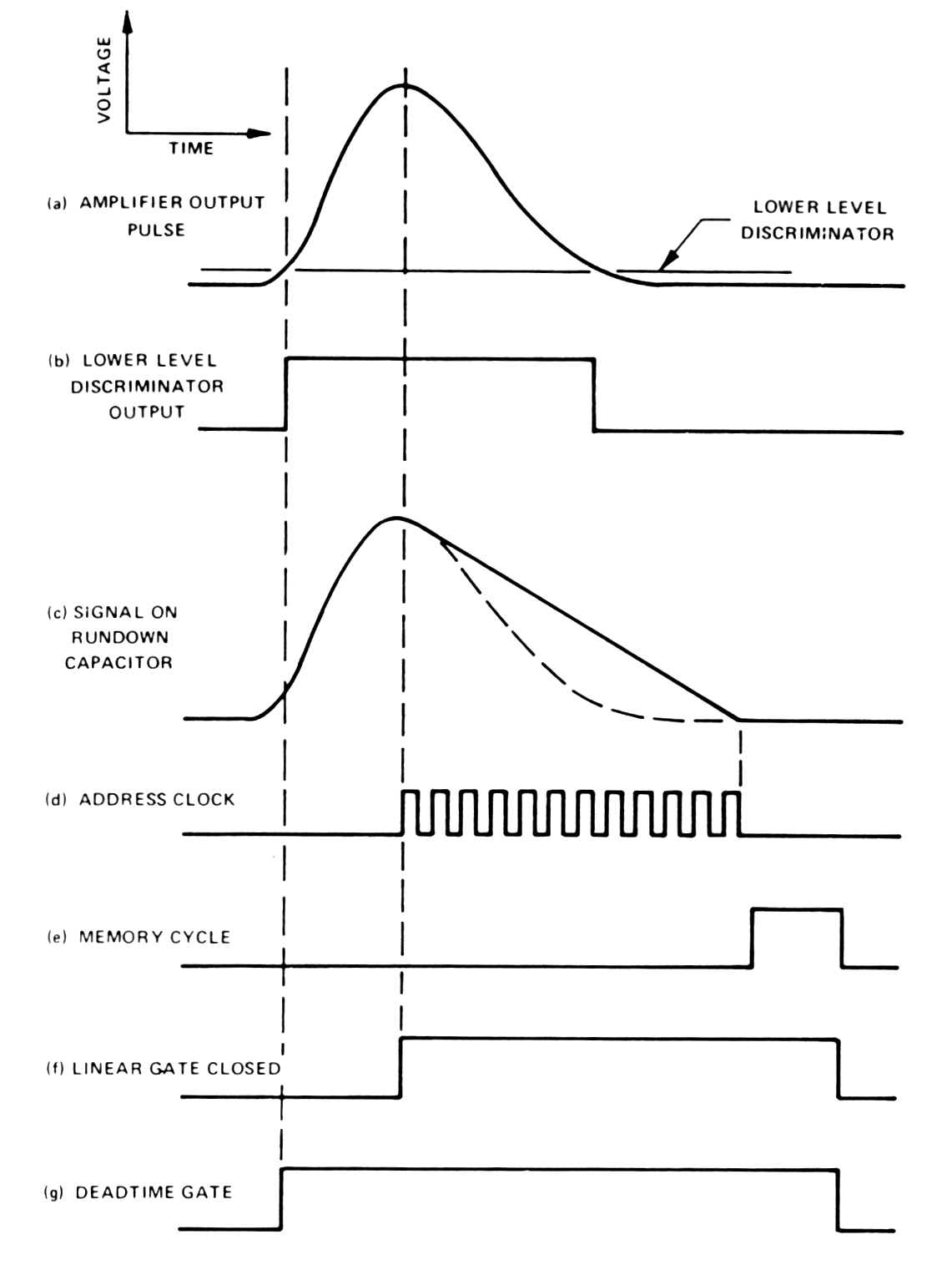 |
Fig. m-59 Signals in the Wilkinson ADC during the pulse measurement process. |
- The low level discriminator (according to fig.) is used to recognize the arrival of the pulse => threshold is set above the noise level to prevent ADC from wasting a lot of time analyzing noise.
- Output discriminator's pulse opens the linear gate (LG). => C is connected to input. C is forced to charge up, so that its Uc follows the amplitude of the rising input pulse.
- When the input pulse has reached its maximum amplitude and begins to fall LG is closed and C is disconnected from the input. Uc ~ max amplitude of the pulse.
- Following peak amplitude detection a constant current source is connected to C to cause a linear discharge (rundown) Uc. At the same time, the address clock is connected to address counter and the clock pulses are counting for the duration of C discharge.
- When the Uc reach zero, the counting stops. Since the time for linear discharge of C is proportional to the original pulse amplitude, the number Nc recorded in the address counter is also proportional to the amplitude.
- During the memory cycle the address Nc is located in the memory and +1 count is added to contents of that location. The value of Nc is usually referred as the channel number.
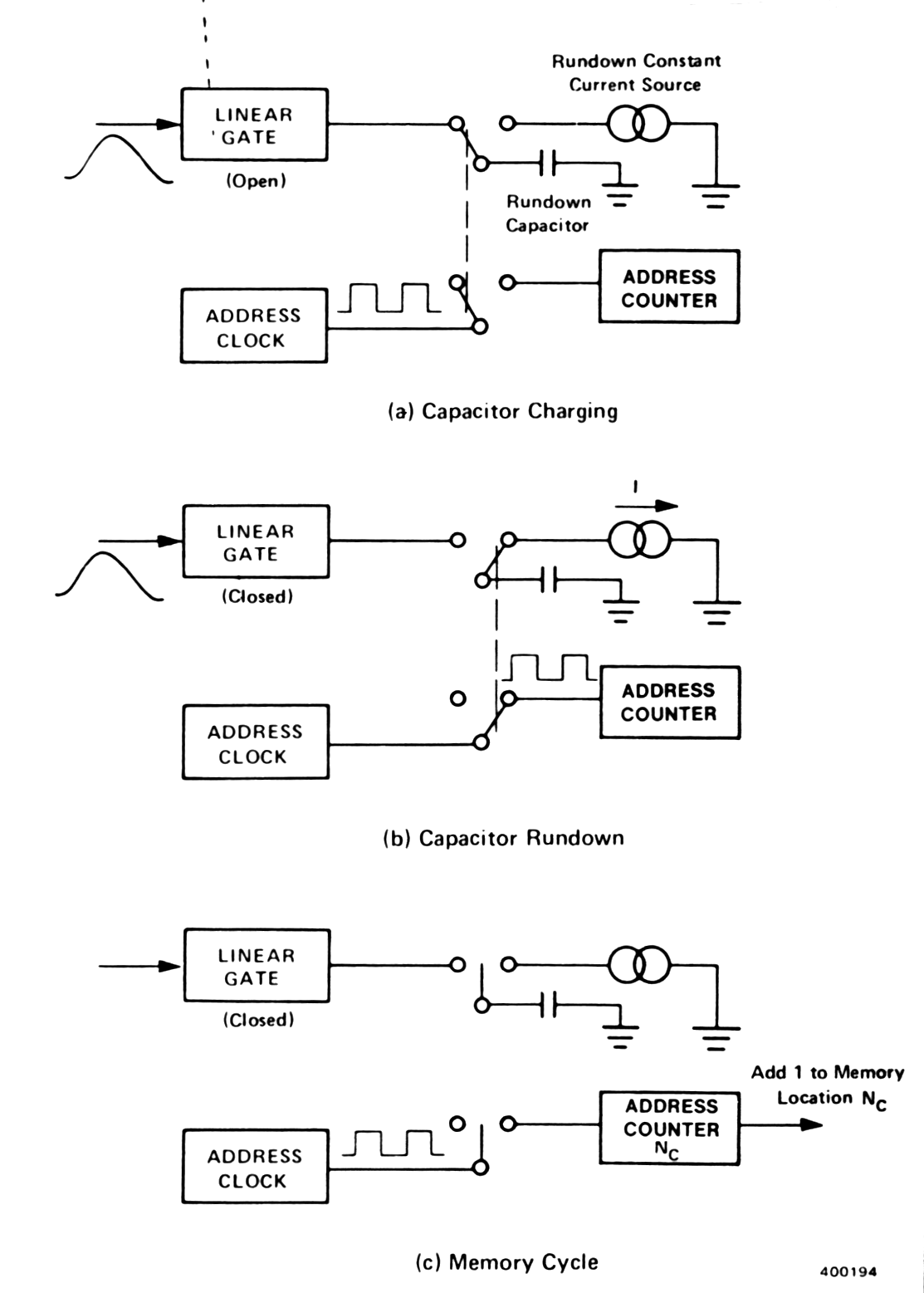 |
Fig. m-60 Operation of the Wilkinson ADC during the tree stages of pulse amplitude measurement:
|
| Sliding scale linearization |
The problem of non adequate DNL of successive-approximation ADC is solved by adding the sliding scale linearization (coarse / fine).
After each pulse is analyzed, the 8 bit-counter is incremented. This results in analog voltage being added to the analog input signal before analysis by the successive approximation ADC .
If the number in the 8 bit counter is m, this results in the successive approximation ADC reporting the analysis m-channels higher then normal. By digitally subtraction on m at the output of the successive approximation ADC, the digital representation is brought back to its normal value.
As the 8-bit counter increments through its
range after each input pulse, it averages the analysis of each pulse
height over 256 adjacent channels in the successive approximation ADC.
This reduces DNL < 1%.
 |
| Fig. m-61 The succesive -approximation ADC with sliding scale linearization. |
Advantage: low DNL and short
conversion time independent of the pulse amplitude. Conversion times in
the range from 2 - 20ms are available with ADC ranging from 1000 to 16 000
channels.
| Timing measurements |
- time relationship between 2 events.
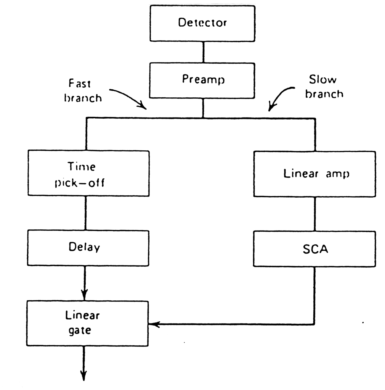 |
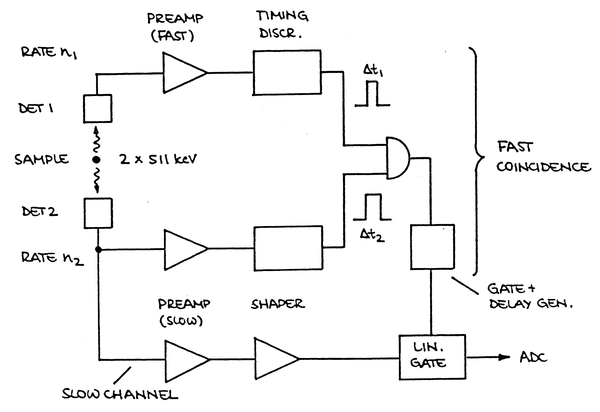
| Fig. m-64 A simple "fast-slow"pulse processing system in which a "slow"amplitude branch is used inly those fast timing pulses that correspond to events of a predetermined amplitude set by the SCA window. |
 |
 |
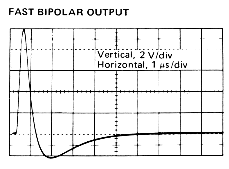
| Fig. m-65 Example of possible output pulses from preamplifier:
|
| Time derivation methods |
Two general types of time derivation methods called "fast" and "slow" timing are characterized by the ways in which the signal is derived and by the result obtained.
Fast timing method - unaltered signals are generated directly at the detectors or signals that have been shaped specifically for timing.
Slow timing signal are derived from
a linear pulse that has been shaped for optimum energy spectroscopy,
using integrating time constants of the order of 0.25 to 10 ms. They are generated from
the output of spectroscopy amplifier by an instrument such as an
integral discriminator or a timing single channel analyzer. Slow timing
signals are used for coincidence experiments, for gating of linear
energy signals, and for gating a desired range of fast-timing signal.
Fast - slow coincidence.
Accept timing pulse only from events that
are in limited energy range.
Exploit superior energy resolution of slow
channel while retaining fast timing capability of wide-band fast channel.
Problem of correct timing
measurements is to obtain a logic signal that is precisely related in
time to event.
| Timing measuremnts |
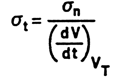
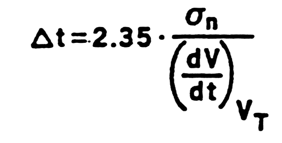
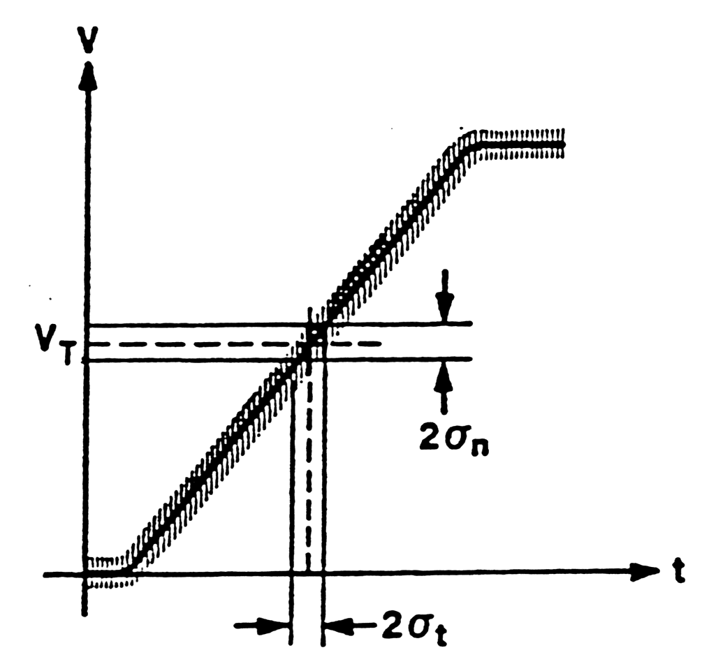
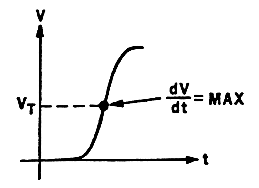
- Time resolution not deterninated by signal-to-noise, but by slope-to-noise ratio Dt.
 |
 |
 |
 |
| Fig.
m-66 Time resolution vs. electronic noise |
Fig. m-67 Optimum trigger level. |
- Increase system bandwidth means:
| noise ~ (fmax)0.5, | (for white noise) |
| dv/dt ~ 1/tr ~fmax | (but not beyond dv/dt of signal) |
- Important applications
| a) | Time of flight (mass of particles, positron measurements in PET, etc); |
| b) | Coincidence measurements (select events, suppress background); |
- Typical results:
| a) | Heavy ion time of flight: Dt=50ps FWHM (noise limited); |
| b) | 60Co: plastic scintillator - plastic scintillator: Dt=200ps FWHM (detector limited); |
| c) | 60Co: plastic scintillator - NaI(Tl): Dt=1ns (detector limited); |
| d) | 60Co: plastic scintillator - Ge(Li): Dt=2-5ns (detector limited); |
| Fast-time pick-off signal from input pulse |
Methods to generate fast-time pick-off signal from input pulse
- Leading - Edge Timing;
- Bipolar pulse and crossover timing;
- Constant - fraction timing;
- Amplitude and Rise - Timing Compensated Timing.
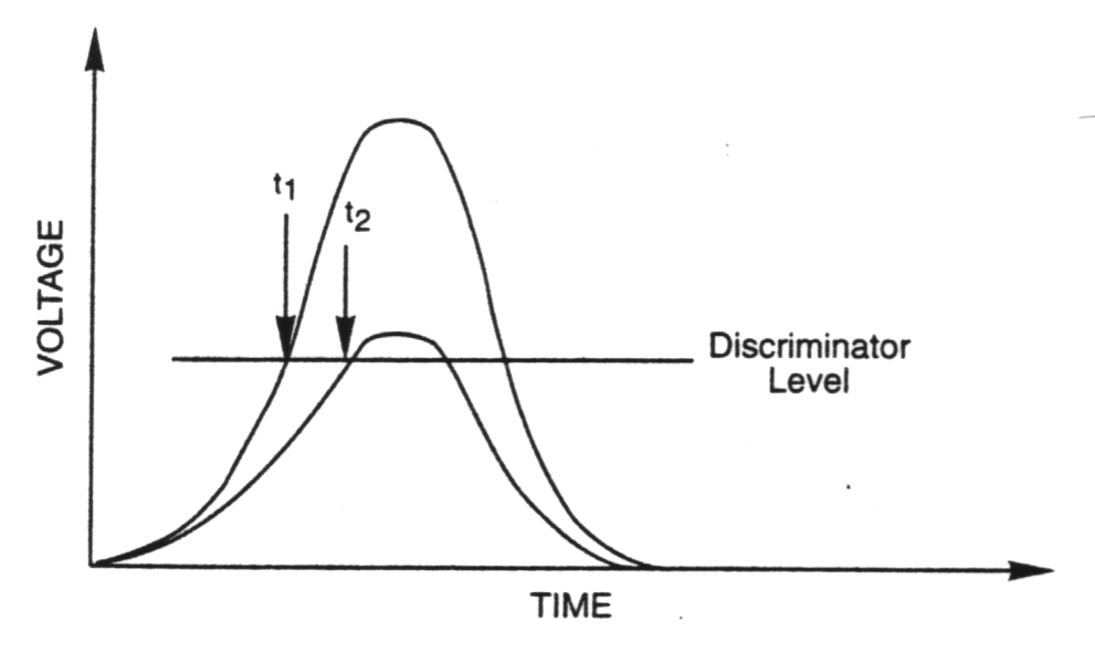
| Leading - Edge Timing |
Drawback: Time of occurrence of
output pulse function of amplitude and rise time => jitter, walk.
Jitter depends on the noise amplitude and the slope of the signal at the
threshold level.
 |
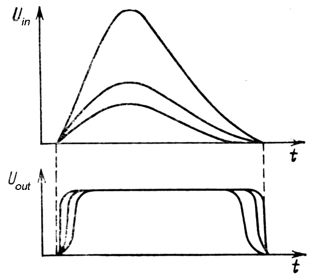 |
Fig. m-68 Leading edge timing. |
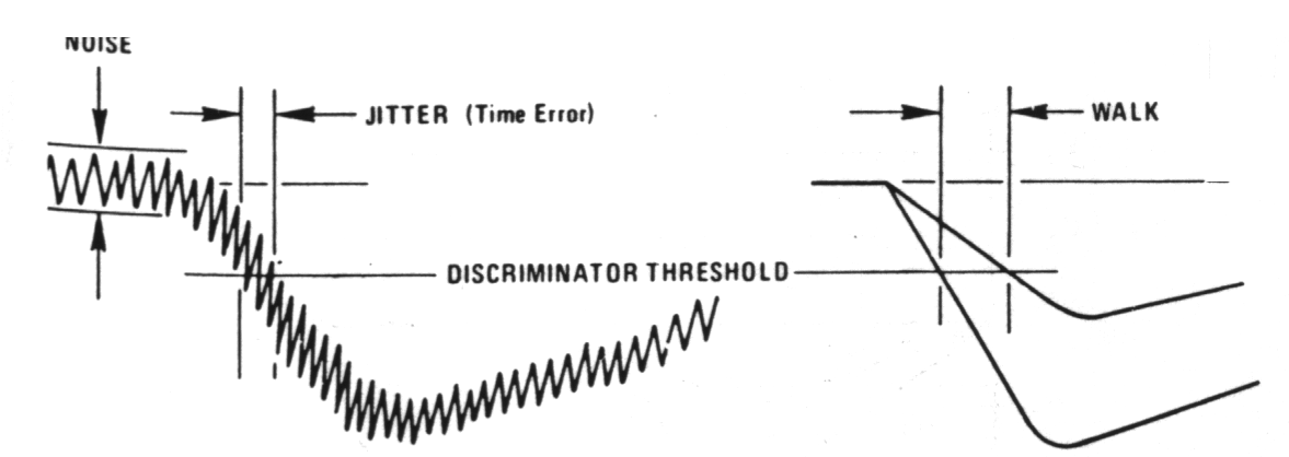 |
Fig. m-69 Jitter and walk in leading-edge time derivation. |
|
Three important sources of error can occur in time pick-off measurement:
- Walk - time movement of the output due to variation in the amplitude of the input impulse (large volume Ge - variations in shape -> dependent charge transition time.
- Drift - long - term timing error by aging, temp. variation.
- Jitter - timing uncertainty of pick-off signal influenced by noise in the system and by statistical fluctuations of the signals from detector.
- in scintillation / photomultiplier (PMT) timing systems, jitter is influenced by the variation of generation rate of photons in the scintillator medium, the transit time variation of the photo-electrons in the PMT, and the gain variation of the PMT.
- In silicon charged particle detectors, jitter is influenced by the leakage current, variations in the detector capacitance, and preamplifier rise time.
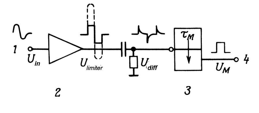
| Bipolar pulse and crossover timing |
Method is based on the fact that the
zero-crossing point in a bipolar pulse is very nearly independent on
pulse amplitude, but after amplification with limiting and sequential
shaping walk and jitters yet occurs. Either double delay shaped pulse or
CR shapping may be used, but the former provide better timing
resolution. For purpose zero cross detector a special type of
discriminator is used.
 |
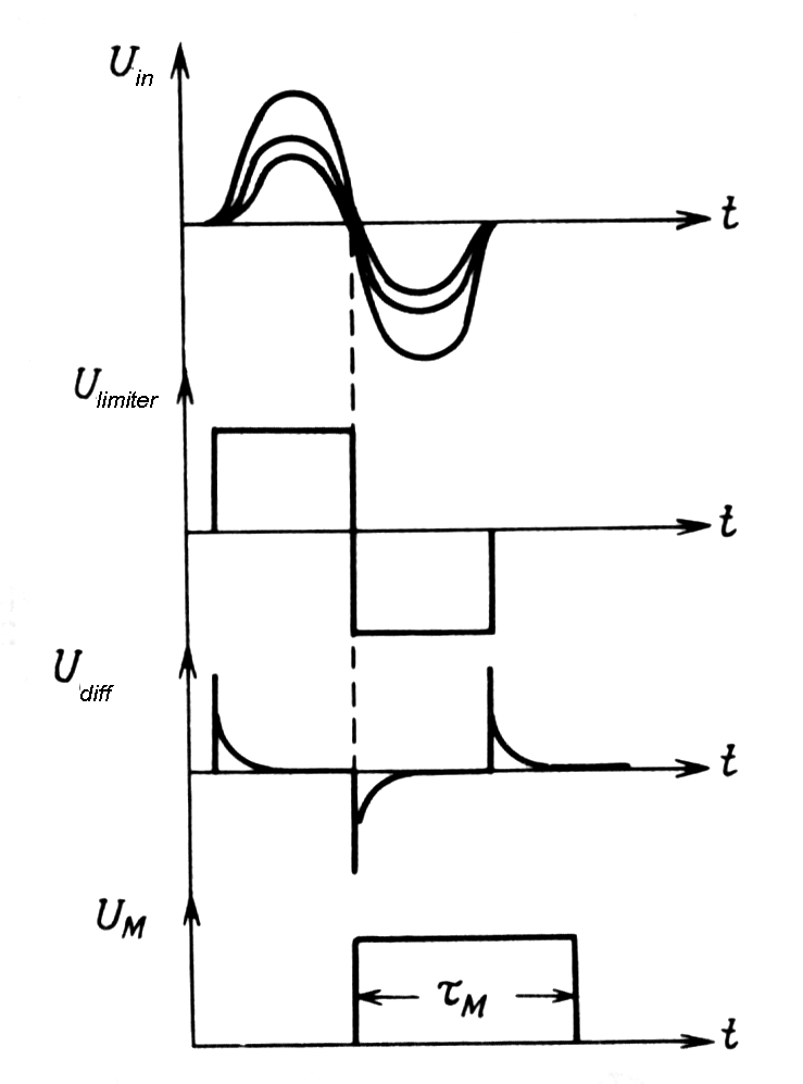 |
Fig. m-70 The principle of zero cross detector:
|
This pulse shaping essentially eliminates amplitude - dependent walk with the uniform rise time.
At the bipolar pulse and crossover timing
method occurrence of the output signal is precisely related to the
occurrence of the detected event and is independent of the "slow" rise
time of the input pulse.
 |
|
| Fig. m-71 The principle of bipolar pulse and crossover timing method | |
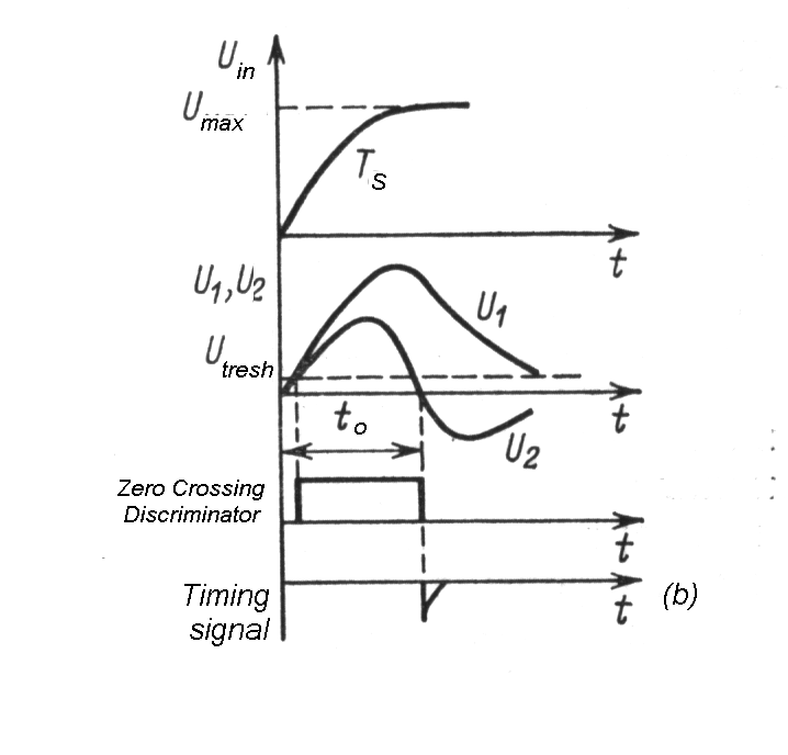 |
Fig. m-72 The bipolar pulse and crossover timing method is suitable for "slow" scintillator (e.g. NaI(Tl) with flash time constant Ts~0,5ms) in which timing associated on rise pulse time is problematical.
|
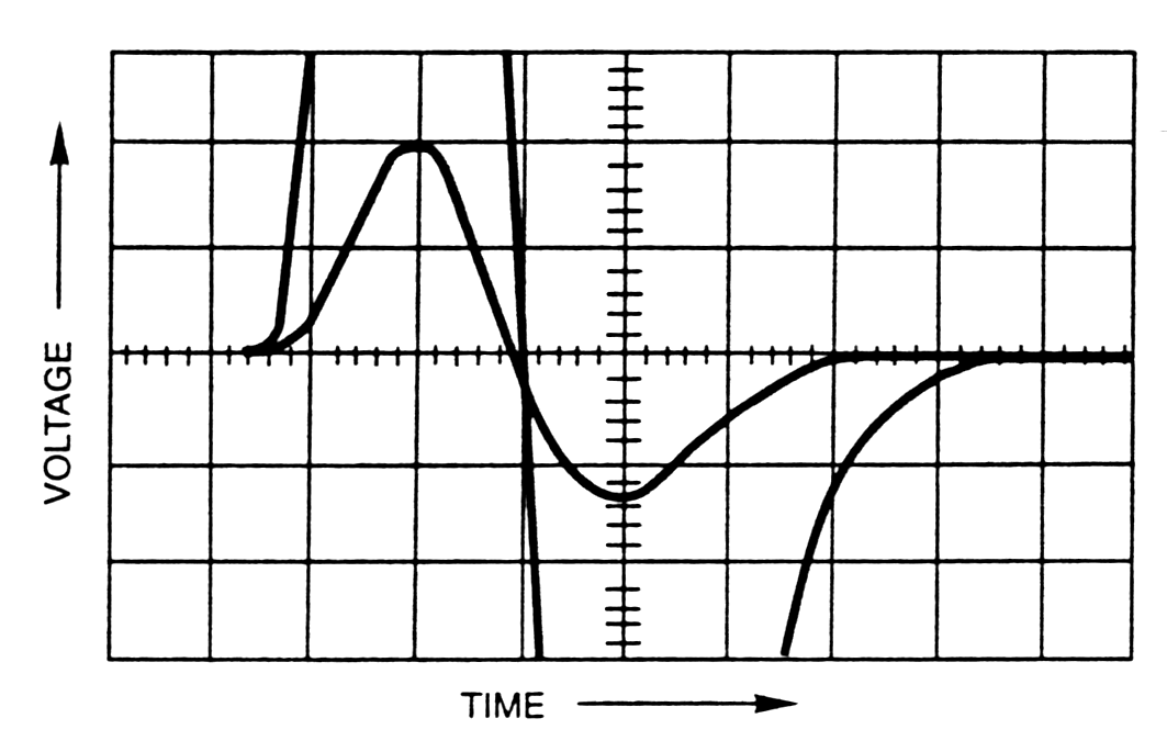 |
Fig. m-73 Bipolar pulses and crossover timing - case height and low pulse amplitude. |
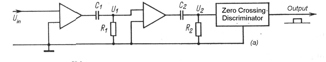
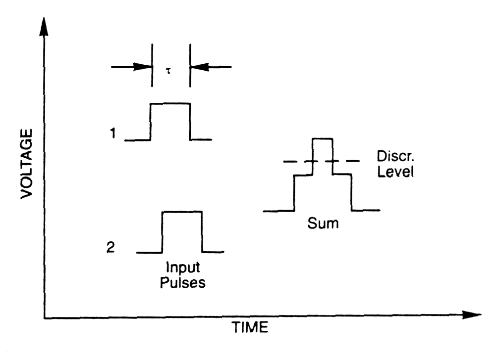
| Constant - fraction timing (CF discriminator) |
The input signal (referring to next
figures) is split into 2 parts: One part is attenuated to a fraction f
of the original amplitude and inverted. And the other part of the signal
is delayed .
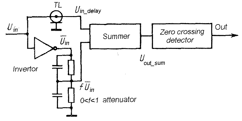 |
Fig.
m-74a The principle of constant - fraction timing (TCF) method. |
(The delay is selected so that the optimum fraction of the delayed signal occurs at the peak amplitude of the attenuated signal). Then a zero crossing is detected and used to produce output logic pulse.
Walk + jitter minimized by proper
adjustment zero - crossing reference selection at attenuating factor +
delay
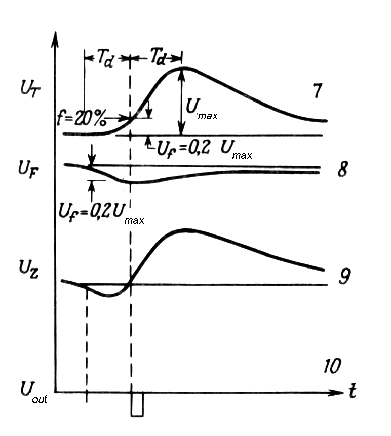 |
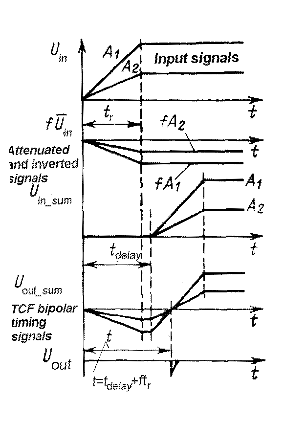 |
| Fig. m-74b 7 - input signal 8 - attenuated input 9 - constant- fraction signal 10 zero-crossing time signal |
Fig. m-74c Example of various pulse hights.
|
| Amplitude and Rise - Timing Compensated Timing |
Amplitude and Rise - Timing Compensated (ARC) timing is used when the input signal has a wide range of rise times.
ARC - special case of constant-fraction
timing, in which the delay is much shorter. ARC timing can
compensate rise time and amplitude variations of the input signal.
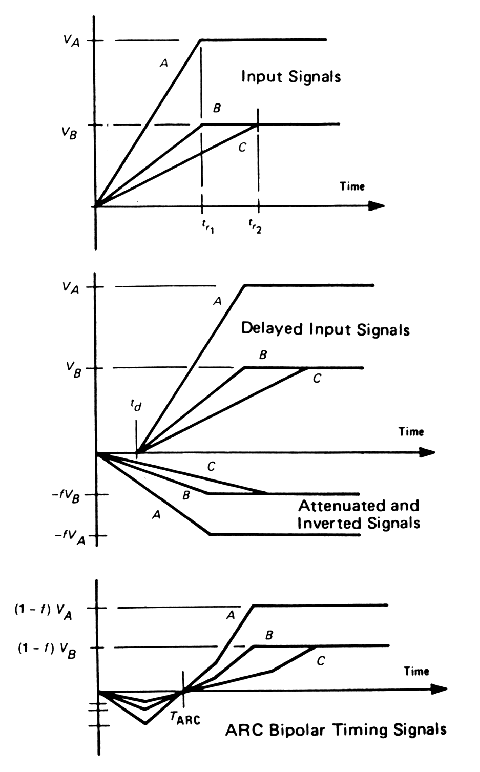 |
Fig. m-75
Signal formation for ARC timing. |
| Concidence system |
determines if 2 events occurs within a
certain fixed period ( with confidence due to uncertainties associated
with the statistical nature of the process, jitter, walk, drift.
 |
 |
| Fig. m-76 Coincidence pulses | Fig. m-77 Logical AND example |
Resolving time - period of time tr in which the 2
input pulses can be accepted (the electronic resolving time determined
by the width of 2 pulses).
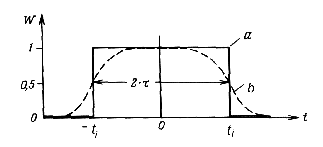 |
Fig. m-78 Resolving time curve. |
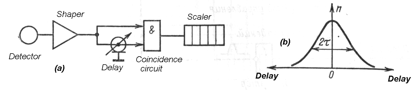 |
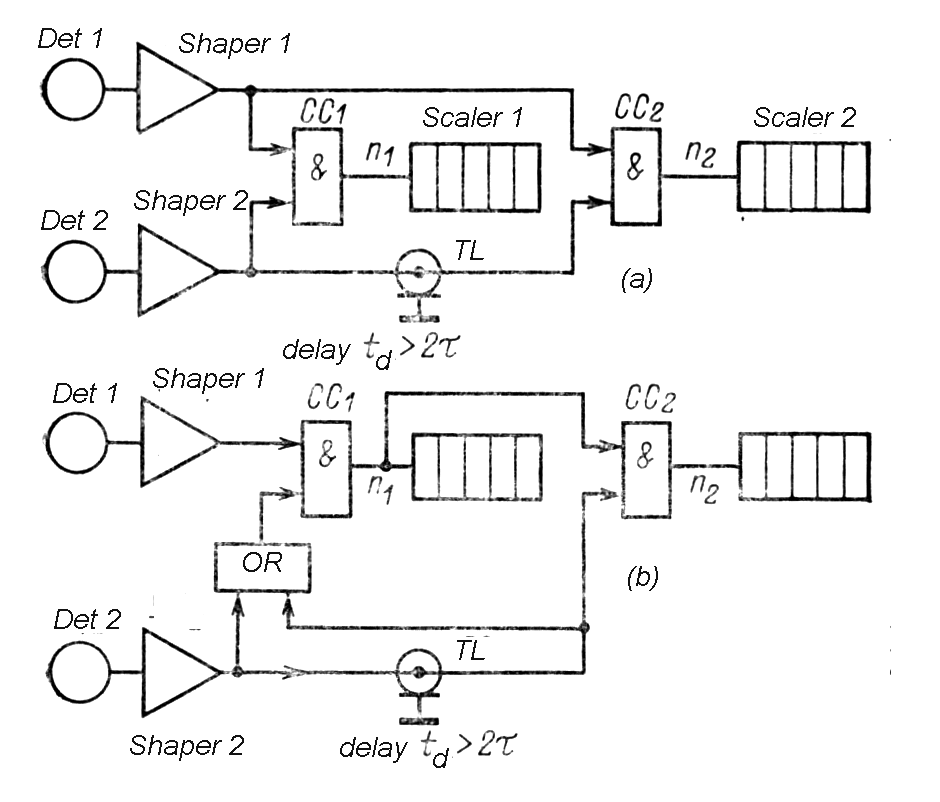
Fig. m-79a Self coincidence method |
 |
Fig. m-79b Resolving time measuremnt on particle beam. |
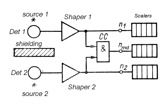
Coincidence circuits produce logic
output pulses when the input pulses occur within the resolving time
window. Since detector events occur at random times, accidental
coincidences can occur between 2 pulses, which produce background in the
coincidence counting. The rate of random coincidence is given
by
| (2)Nrnd = N1*N2*(2tr) | |
| Where N1 and N2 are counting rate in detector 1 and 2 per s; | |
| or generally for m input coincidence circuit with resolving time tr: | |
| (m)Nrnd=m*N1*N2*…. Nm*(2tr)(m-1) |
The best way to reduce random coincidences is to make resolving time as small as possible. However the resolving time cannot be reduced bellow the amount of time jitter the detector pulses without losing true coincidence, so the type of detector determines the minimum resolving time usable.
In order to properly operate the system a
delay curve is obtained in which coincidences are measured as a
function of relative delay between 2 detectors. In ideal case of no time
jitter in either detector a plat region curve is obtained.
 |
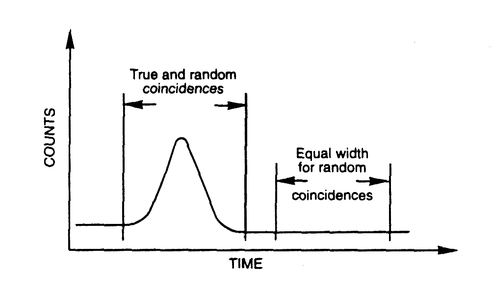 |
| Fig. m-80b Determination of resolving time - tr = (2)Nrnd/(2*N1*N2*) based on measurement of random coincidence Nrnd number. | |
Typical resolving time ~10 ns for energy
range 0,1 to 1 MeV. Shorter resolving time possible for plastic
scintillators, for Si-detectors ~1 ns.
 |
|
 |
| Fig.
m-82 Example of background suppression in
positron annihilation measurement. Chance coincidence rate: nc=n1n2(Dt1+Dt2)~10-4 s-1 (when we suppose that n1=n2=107s-1,Dt1=Dt2=1ns). |
| Time intervals measuremnts |
| A) | Start – Stop Method |
– the basic Method for conversion
t->T->D (time t to interval T to digit D).
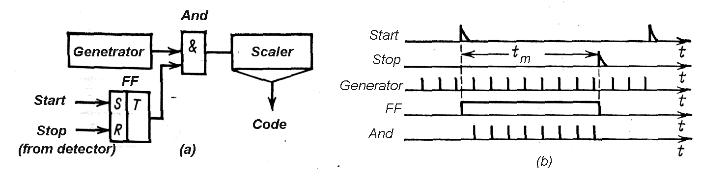 |
| Fig. m-83 The principle of Start-Stop Method of time interval measurement. |
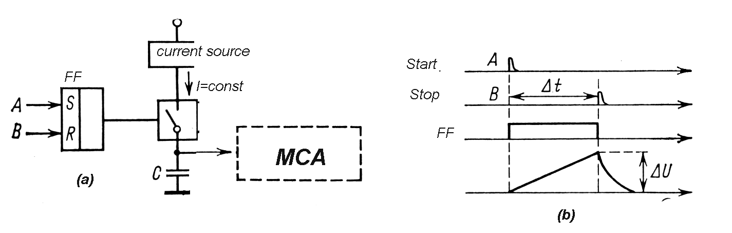
| B) | TAC – the conversion t->A with MCA |
MCA -(Multi channel Analysator)
| B1) | Start – Stop method with integrating capacitor for t->A conversion |
|
|
Fig. m-84 The principle of start-stop time- amplitude (t --> A) conversion method. The method is suitable especially for nanoseconds time intervals, where direct start-stop method is hardly applicable. |
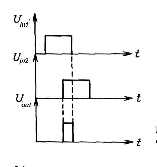
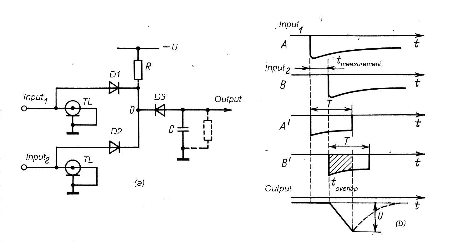
| B2) | Coincidence circuit method with pulse overlap |
|
|
Fig. m-85 Time - amplitude (t-->A) conversion method based on input pulses overlap. When T is duration of the shaped pulse then measured time interval tmeasurement: |
|
The method is suitable for fast rise time pulses, which were shaping by delay line clip. |
| B3) | TADC – the conversion t-->A-->T-->D |
(time t to amplitude A to interval T to digit D conversion). The very short intervals can be:
- expanded or
- more exactly measured with interpolation method.
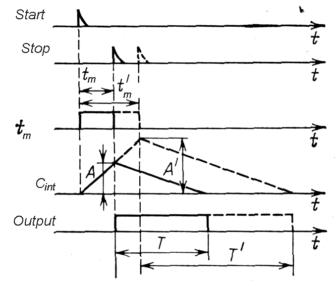
a) Time expander (expands ns duration intervals to us intervals). Capacitor Cint is quickly charging during measured time interval tm (by great current –for example 20mA) and after receiving stop pulse is discharging slowly during time interval T (by low current –for example 80uA). The time expanded by factor T/tm is measured by classic start - stop method (as in paragraph A). Advantage: better linearity of conversion then in previously mentioned methods, while the same capacitor Cint is used in both parts of conversions.
|
|
Fig. m-86 The principle of the time- amplitude-time (t-->A-->t) conversion. |
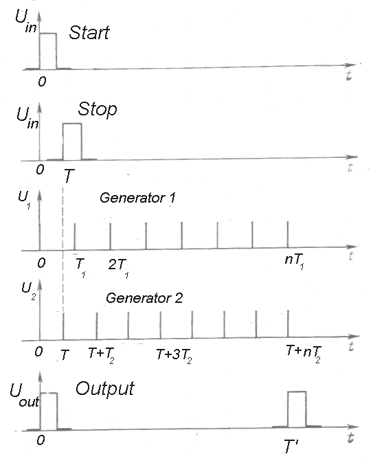
b) Nonius (Vernier) method -exact interpolation method
Start pulse initiates generating pulses at rate T1. After time interval T (which is point of our interest), the Stop pulse begins generating pulses at rateT2. (The difference of rates T1-T2 is about 1%). When a coincidence after n pulses occurs: T’=nT1=[T1/(T1-T2)]T=kT.
The conversion coefficient k=T1/(T1-T2) allows to measure (in microsecond) the original nanosecond duration interval.
Fig. m-87
The principle of the Nonius method
T - interval, which is point of our interest
T' - exactly measured duration, which is proportional to T.
| Back to menu |